Solution
ID: past-exam-of-the-mphil-in-micro-and-nanotechnology-enterprise-course-of-the-university-of-cambridge/2023/paper-1/section-b/9/v/solution
Past exam of the MPhil in micro- and nanotechnology enterprise course of the University of Cambridge 2023 Paper 1 Section B 9 v Solution by  Codex 0 2026-10-20
Use equal-width rectangular contact windows in a row with several different edge-to-edge spacings. For positive-resist lift-off, the future metal pads correspond to clear windows in an otherwise chrome-covered mask: exposure removes resist there, and the unexposed background retains resist beneath unwanted metal.
For ordinary ohmic transmission line contact measurement, a conducting strip or isolated mesa of width connects adjacent pads. Measure several spacings so thatThe intercept separates two contact contributions from the sheet-resistance slope. Large enough pad length relative to the transfer length is needed for the simplest contact-resistivity extraction.
Prepare separate arrays on the appropriate surfaces: annealed source/drain metal on the n+ cap, and gate metal on cap-removed AlGaAs. A Schottky gate is nonlinear, so its interface cannot be assigned an ohmic zero-bias contact resistivity merely by fitting the same straight line. Use bias-dependent current–voltage or differential-contact analysis, accounting for the two rectifying contacts.
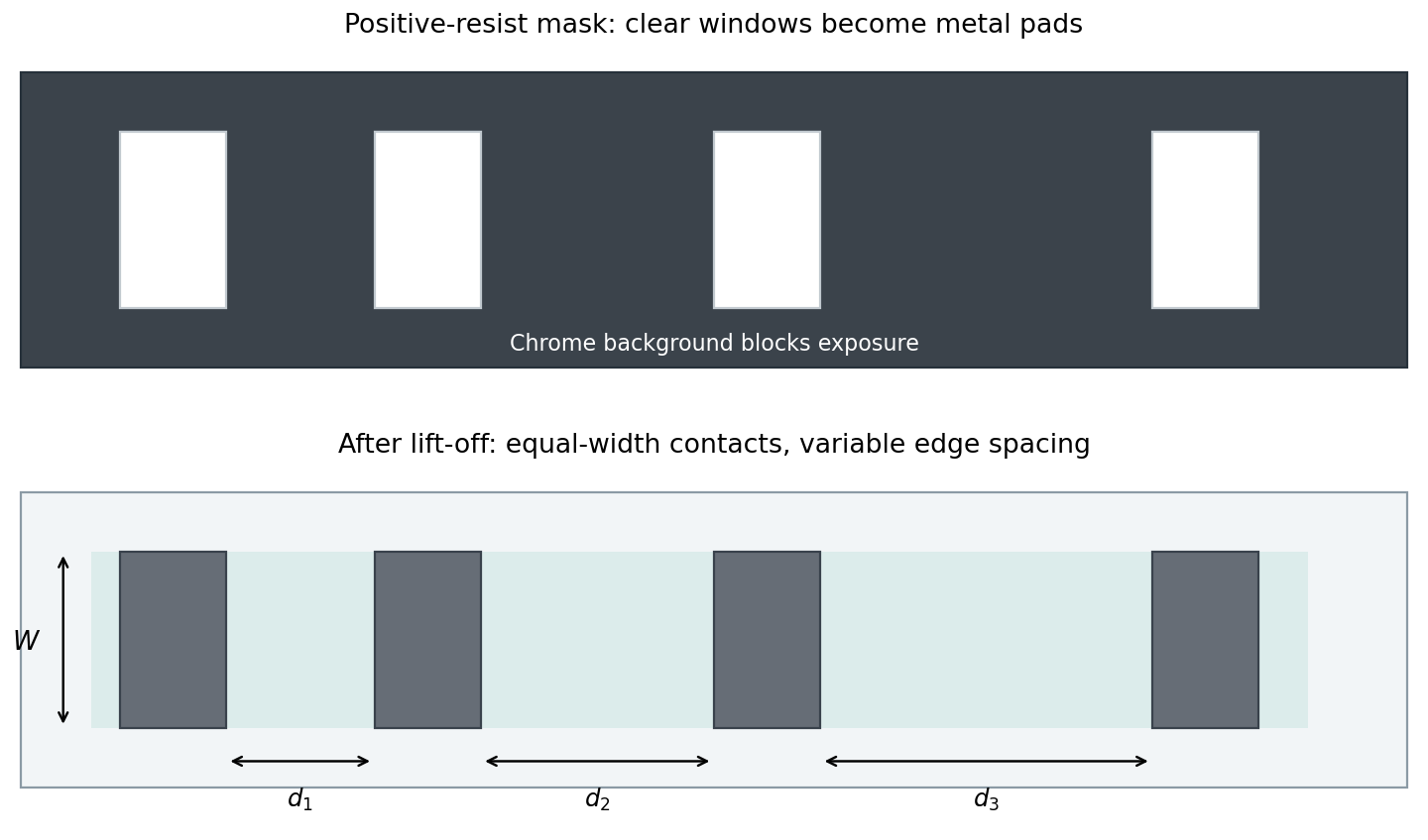
Positive-resist lift-off mask and variable-spacing contact array
. Original schematic. Pale windows in the dark chrome background define future metal pads. The resulting equal-width pads have different edge spacings. Ohmic TLM analysis and bias-dependent analysis of a Schottky contact require distinct electrical models. Details.
New to topics? Read the docs here!