Topics (318k) Articles (329k) Users (388) Discussions (237) Comments (383) Files (10k) New article

Ion implantation-induced nanoparticle formation refers to the process of creating nanoparticles within a material by implanting ions at high energies. This technique is often utilized in materials science and semiconductor fabrication to modify the properties of solids at a nanoscale level. ### Key Aspects of Ion Implantation-Induced Nanoparticle Formation: 1. **Ion Implantation Process**: - Involves shooting ions (charged particles) into a target material, which can be a semiconductor, metal, or insulator.
Ion beam deposition (IBD) is a physical vapor deposition (PVD) technique used to deposit thin films of materials onto substrates. It involves the use of a focused beam of ions—typically generated by an ion source—that is directed at a target material. The key steps of the process are as follows: 1. **Ion Generation**: Ions are generated from a gas (often noble gases like argon) using an ion source, which creates a plasma of charged particles.
Ion beam-assisted deposition (IBAD) is a materials deposition technique that combines traditional physical vapor deposition (PVD) methods with an energetic ion beam to enhance the properties of thin films. In this process, a deposition material—typically a metal, semiconductor, or dielectric—is evaporated or sputtered onto a substrate, while simultaneously directing a beam of ions (which can be inert gases like argon) at the growing film surface.
IBM (International Business Machines Corporation) is a multinational technology and consulting company known for its work in fields such as computing, artificial intelligence, cloud computing, and quantum computing. However, if you are referring to "IBM" in the context of "atoms," this is likely a misunderstanding or a need for clarification. In the field of atomic and molecular physics, there is a concept known as "IBM," which stands for the **Interacting Boson Model**.
Graphite-like zinc oxide nanostructures refer to a specific type of zinc oxide (ZnO) that exhibits structural and electronic properties similar to those of graphite. These nanostructures can exhibit unique properties due to their two-dimensional (2D) nature and are often synthesized in forms such as nanosheets, nanoplates, or other layered structures.
Gold nanocages are nanoscale structures made primarily from gold that have a hollow, cage-like architecture. They are a type of gold nanostructure that exhibits unique physical and chemical properties due to their size, shape, and surface characteristics. Here are some key features and aspects of gold nanocages: 1. **Structure**: Gold nanocages typically have a porous structure with a hollow interior, resembling a cage.
Fluorescence intermittency, often referred to as "blinking," is a phenomenon observed in fluorescent molecules or nanoparticles where their fluorescence emission fluctuates between periods of brightness and darkness. This behavior is particularly common in single molecules or small clusters of molecules, such as quantum dots and certain organic fluorophores.
A "comb drive" typically refers to a type of microelectromechanical system (MEMS) actuator that is used for precise positioning and manipulation of microscale components. Comb drives are characterized by their structure, which resembles a series of interdigitated comb-like fingers or plates. ### How Comb Drives Work: 1. **Electrostatic Actuation**: The fundamental principle behind comb drives is electrostatic actuation.
In physics, a "cluster" typically refers to a group of atoms, molecules, or particles that are bound together. The term can be used in various contexts, including the following: 1. **Atomic Clusters**: These are small aggregates of atoms that can exist in a free state or as a part of a material. Their properties can differ significantly from those of bulk materials due to the effects of surface area and quantum mechanics.
The Center for Probing the Nanoscale (CPN) is a research facility based at Stanford University focused on advancing the understanding of nanoscale materials and their properties. It is known for its interdisciplinary approach, bringing together researchers from various fields such as physics, chemistry, materials science, and engineering to explore and develop new technologies at the nanoscale.
A carbon nanohoop is a nanostructure composed of carbon atoms arranged in a cyclic manner, resembling a hoop or ring-like structure. It is part of a class of materials known as nanocarbon, which also includes fullerenes, carbon nanotubes, and graphene. Carbon nanohoops are characterized by their unique geometries and properties, which make them of interest in various fields, including materials science, nanotechnology, and organic electronics.
Bulk micromachining is a manufacturing process used primarily in the microfabrication of devices and structures from a bulk material, typically silicon. This technique is part of the broader field of micromachining, which involves the design and production of micro-scale components and systems, often for applications in MEMS (Micro-Electro-Mechanical Systems), sensors, and actuators. In bulk micromachining, the material is selectively removed from the bulk substrate to create three-dimensional microstructures.
Ag-Sb2S3 refers to a compound consisting of silver (Ag), antimony (Sb), and sulfur (S), specifically silver antimony trisulfide. Its chemical formula can be written as AgSb2S3. This compound is part of a family of materials known as sulfides and has been studied for various applications, including electronics, semiconductors, and potential use in photovoltaic devices.
The term "800 nm process" typically refers to a semiconductor manufacturing technology that features a minimum feature size of 800 nanometers (nm). This size indicates the smallest dimension that can be reliably fabricated on a semiconductor chip. In the context of integrated circuits (ICs), as technology has advanced, the trend has been toward smaller feature sizes to enable more components to fit on a single chip, improving performance, efficiency, and functionality.
The term "6 µm process" refers to a semiconductor manufacturing technology that has a minimum feature size of 6 micrometers (µm) which is equivalent to 6,000 nanometers. This process is part of a family of technologies used to fabricate integrated circuits (ICs), where the size of the features on the chip (such as transistors, resistors, and capacitors) measures 6 µm or larger.
The term "600 nm process" refers to a semiconductor manufacturing technology that uses a lithographic feature size of 600 nanometers (nm) for the fabrication of integrated circuits (ICs). This process node is part of the ongoing trend in the semiconductor industry, where smaller feature sizes typically result in more transistors being packed onto a chip, which can lead to improved performance, reduced power consumption, and decreased costs per transistor.
The term "3 µm process" refers to a specific technology node in semiconductor manufacturing where the features of integrated circuits (ICs) are produced with a minimum half-pitch of 3 micrometers (µm) or 3000 nanometers. This measurement typically indicates the smallest half-width of conductive lines and spaces on the chip. The process technology encompasses various stages, including design, fabrication, and testing.
The term "350 nm process" refers to a semiconductor manufacturing process technology that uses a minimum feature size of 350 nanometers (nm). This indicates the smallest half-pitch of contactable features that can be reliably produced on a silicon wafer during the fabrication of integrated circuits (ICs). ### Key Points About 350 nm Process Technology: 1. **Process Node**: Each "process node" (like 350 nm) is a step in the evolution of chip manufacturing.
The term "250 nm process" refers to a semiconductor manufacturing technology that fabricates integrated circuits (ICs) with features that are approximately 250 nanometers (nm) in size. The "process" indicates the specific technology node or generation of fabrication techniques used to create these microchips.
The term "1 µm process" refers to a semiconductor manufacturing technology that has a minimum feature size of 1 micrometer (µm), or 1000 nanometers (nm). In the context of integrated circuit (IC) fabrication, the "process" describes the series of steps and techniques used to create electronic circuits on silicon wafers.
Pinned article: Introduction to the OurBigBook Project
Welcome to the OurBigBook Project! Our goal is to create the perfect publishing platform for STEM subjects, and get university-level students to write the best free STEM tutorials ever.
Everyone is welcome to create an account and play with the site: ourbigbook.com/go/register. We belive that students themselves can write amazing tutorials, but teachers are welcome too. You can write about anything you want, it doesn't have to be STEM or even educational. Silly test content is very welcome and you won't be penalized in any way. Just keep it legal!
Intro to OurBigBook
. Source. We have two killer features:
- topics: topics group articles by different users with the same title, e.g. here is the topic for the "Fundamental Theorem of Calculus" ourbigbook.com/go/topic/fundamental-theorem-of-calculusArticles of different users are sorted by upvote within each article page. This feature is a bit like:
- a Wikipedia where each user can have their own version of each article
- a Q&A website like Stack Overflow, where multiple people can give their views on a given topic, and the best ones are sorted by upvote. Except you don't need to wait for someone to ask first, and any topic goes, no matter how narrow or broad
This feature makes it possible for readers to find better explanations of any topic created by other writers. And it allows writers to create an explanation in a place that readers might actually find it.
Figure 1. Screenshot of the "Derivative" topic page. View it live at: ourbigbook.com/go/topic/derivativeVideo 2. OurBigBook Web topics demo. Source. - local editing: you can store all your personal knowledge base content locally in a plaintext markup format that can be edited locally and published either:This way you can be sure that even if OurBigBook.com were to go down one day (which we have no plans to do as it is quite cheap to host!), your content will still be perfectly readable as a static site.
- to OurBigBook.com to get awesome multi-user features like topics and likes
- as HTML files to a static website, which you can host yourself for free on many external providers like GitHub Pages, and remain in full control

Figure 2. You can publish local OurBigBook lightweight markup files to either OurBigBook.com or as a static website.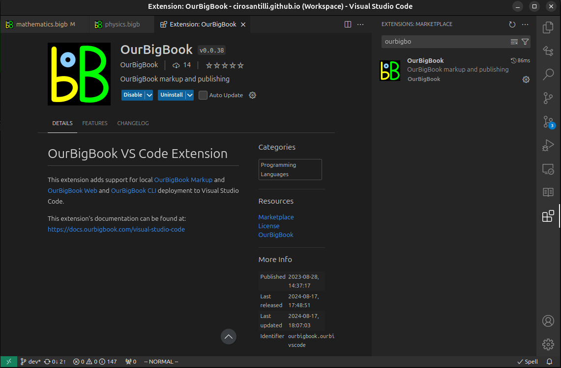
Figure 3. Visual Studio Code extension installation.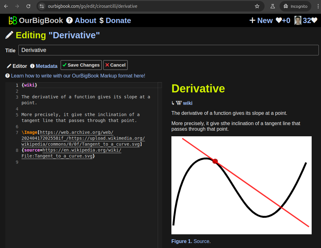
Figure 5. . You can also edit articles on the Web editor without installing anything locally. Video 3. Edit locally and publish demo. Source. This shows editing OurBigBook Markup and publishing it using the Visual Studio Code extension. 
- Infinitely deep tables of contents:
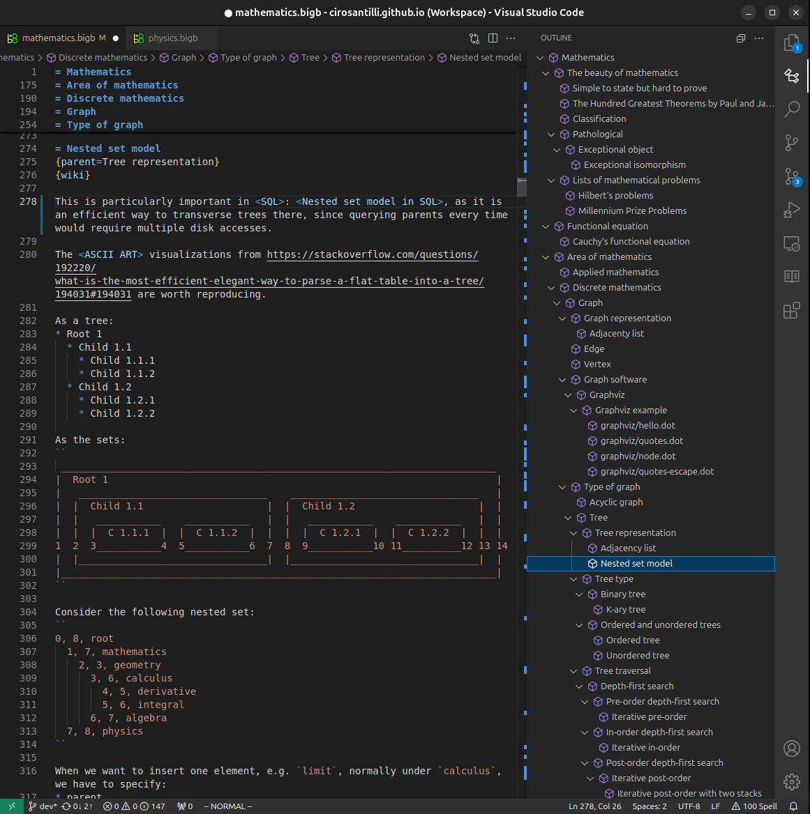

All our software is open source and hosted at: github.com/ourbigbook/ourbigbook
Further documentation can be found at: docs.ourbigbook.com
Feel free to reach our to us for any help or suggestions: docs.ourbigbook.com/#contact