Solution
ID: past-exam-of-the-quantum-condensed-matter-course-of-the-university-of-cambridge/2004/section-b/b9/c/solution
Past exam of the quantum condensed matter course of the University of Cambridge 2004 Section B B9 c Solution by  Codex 0 Created 2026-10-18 Updated 2026-10-20
An n-channel MOSFET has two heavily n-doped source and drain regions in a p-type body, with an insulated gate above the intervening surface. A positive gate voltage first depletes surface electron holes and then induces an electron semiconductor inversion layer. Above threshold this layer connects source to drain. Gate voltage controls the channel charge through the oxide capacitance, while the insulating gate permits a very small steady gate current.
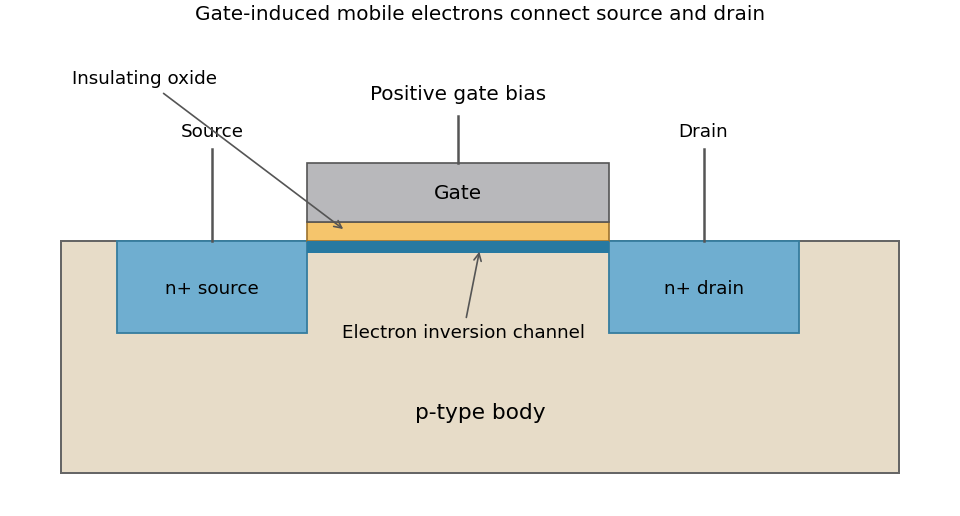

For the long-channel MOSFET current law, let be oxide capacitance per area, channel width and length, and use constant mobility . In the gradual-channel approximation,At larger drain voltage the ideal channel pinches off near the drain and the current saturates atCarriers still flow through the pinch-off region; pinch-off does not mean zero drain current. These formulas neglect channel-length modulation, short-channel effects and velocity saturation. A p-channel device reverses the carrier type and operating polarities. Gate control makes MOSFETs useful as electronic switches and amplifiers.
New to topics? Read the docs here!