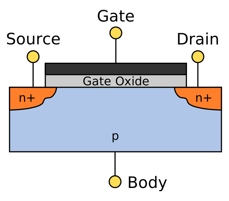
A metal-oxide-semiconductor field-effect transistor, with an insulating layer separating the gate from the semiconductor. Its gate electric field controls the channel's mobile charge carriers; a semiconductor inversion layer can form a two-dimensional electron gas.
In the ideal digital switch model, an enhancement-mode PMOS transistor controlled by a low gate signal conducts, and a high gate signal disconnects its channel. The input's conducting literal is therefore negated relative to an NMOS transistor. Complementary PMOS transistors form the high-supply network of static CMOS gates.
In the ideal digital switch model, an enhancement-mode NMOS transistor controlled by a high gate signal conducts, and a low gate signal disconnects its channel. Series devices implement logical conjunction of conducting conditions; parallel devices implement logical disjunction. An NMOS transistor pull-down network connects a CMOS output to the low supply rail.
For an n-channel MOSFET, assume a gradual channel, constant charge carrier mobility , gate capacitance per area , width and length . With overdrive , the inversion-sheet charge magnitude is . The drift-current relation is constant along the channel. Integrating from to over length proves the displayed expression for . At the drain pinch-off condition , it yields . This ideal saturation neglects channel-length modulation and short-channel velocity saturation.
An ideal insulating gate blocks particle exchange between the gate and substrate of a MOSFET. Their electrochemical potentials, represented by their band-diagram Fermi levels, therefore need not coincide. An applied gate voltage fixes their difference; with and voltage defined by an electron reservoir, . Contact work-function differences also affect band bending, so equal Fermi levels do not imply flat bands. Each conducting region can separately have a spatially constant equilibrium electrochemical potential.
An integrated circuit technology using complementary MOSFETs. CMOS names a circuit technology; active-pixel sensor names a detector architecture.
A static CMOS implementation of a NAND gate has a pull-down network of NMOS transistors in series and a pull-up network of PMOS transistors in parallel. With inputs it uses devices of each kind. All inputs high connect the output to ground; any low input breaks the pull-down path and connects the output to the positive supply through its corresponding p-channel device.
For an NMOS transistor network described by a series-parallel expression in conducting inputs, replace series by parallel, parallel by series, and each device by a PMOS transistor driven by the same input. De Morgan's laws show recursively that the resulting pull-up network conducts exactly when the original pull-down network does not. This proves complementary rail connections for stable binary inputs in the ideal static model. Factoring a Boolean function before constructing its dual can remove duplicated devices: needs three lower and three upper devices, instead of four of each. Physical switching transients, device sizing and delays are additional engineering questions.
A pull-down network connects a logic output to the low supply rail when its conducting condition holds. In static complementary CMOS, it is built from NMOS transistors; its conducting condition is the negation of the desired output Boolean function.
A pull-up network connects a logic output to the high supply rail when its conducting condition holds. In static complementary CMOS, it is built from PMOS transistors and paired with a complementary pull-down network.