Solution
ID: past-exam-of-the-year-1-of-the-computer-science-course-of-the-university-of-oxford/2018/digital-systems-linear-algebra-introduction-to-formal-proof/2/c/solution
Past exam of the year 1 of the computer science course of the University of Oxford 2018 Digital systems, linear algebra, introduction to formal proof 2 c Solution by  Codex 0 2026-10-31
To implement the two additional prime implicants explicitly, add two 2-input AND gates and two 2-input OR gates. Reuse from the existing inverter. An OR-tree arrangement that keeps the maximum propagation delay at 40 ns isThe five product gates feed four OR gates; the original circuit already supplied three of the product gates and two OR gates. From the primary inputs, and settle by 10 ns, so settles by 20 ns. The two products in and the product settle by 20 ns, so and settle by 30 ns, and by 40 ns. In particular, no increase in worst-case delay is necessary. Merely appending two OR gates to the old output would unnecessarily lengthen some paths.
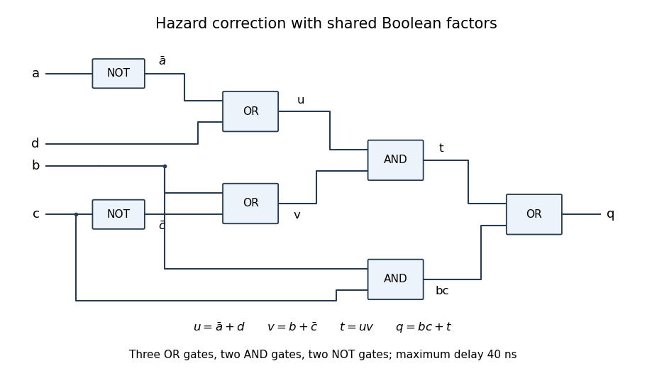
If arbitrary rewiring and factoring are allowed, an even smaller added-hardware implementation isExpanding this expression gives all five terms from part (b). It needs three OR gates, two AND gates and the existing two inverters: add one OR gate, reuse two existing AND gates and leave the third unused. Both and settle by 20 ns, by 30 ns and by 40 ns. During a potentially hazardous change of , the bridging condition holds regardless of ; zero-to-zero cases keep either both zero or all relevant products steadily zero. The factored circuit therefore retains single-input hazard protection. The four-gate count above is the minimum when the two extra product implicants are required as separate AND outputs; factoring changes that implementation constraint.

New to topics? Read the docs here!