Solution
ID: past-exam-of-the-quantum-condensed-matter-course-of-the-university-of-cambridge/2018/section-a/1/b/solution
Past exam of the quantum condensed matter course of the University of Cambridge 2018 Section A 1 b Solution by  Codex 0 2026-10-18
Codex 0 2026-10-18A positive gate voltage attracts Electrons towards the oxide interface of the p-type semiconductor and repels mobile electron holes. The uncovered ionized acceptors form a negatively charged depletion region. Increasing the voltage further creates a thin electron-rich semiconductor inversion layer at the surface. The conduction band and valence band both bend downwards towards the positively biased gate, because an electron's electrostatic energy is .
In an ideal nondegenerate substrate with acceptor density , write and surface potential relative to the neutral bulk. The electron and hole surface densities areThe first change of majority-carrier type occurs at , where . The conventional MOS inversion threshold for appreciable strong inversion isAt threshold the inversion sheet is just developing, while a much thicker depletion region lies between it and the neutral p-type bulk. Inversion does not require the conduction band to cross the Fermi level: the surface can remain nondegenerate.
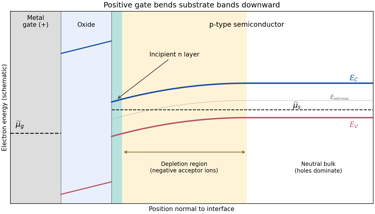

The metal and semiconductor Fermi levels need not be equal. The ideal oxide blocks particle exchange, so the gate and substrate can maintain different electrochemical potentials. In a biased MOSFET, the gate-to-substrate Fermi-level difference is , when the applied voltage is defined in the electron-reservoir convention. Each region can separately be in internal equilibrium. If an external zero-voltage connection instead equilibrates the reservoirs, their Fermi levels coincide, but different work functions can still cause band bending. Here the chemical potential shown in a band diagram is the electron electrochemical potential; the purely chemical contribution alone is not the equilibrium criterion for charged particles.
New to topics? Read the docs here!