How LEDs work by VirtualBrain
. Source. 2021. Good 3d schematics clearly explaining part of the LED electronic package.How are LED Chips and LED Encapsulation is made by Future Linear
. Source. Starts from some level of cut square chips. Still in round wafer form.www.reddit.com/r/Optics/comments/18f6bdt/comment/kcsiook/ mentions:
LEDs are broadband by nature, since the spontaneous emission broadly speaking reflects the overlap of the Fermi distribution and the density of states
Bibliography:
Articles by others on the same topic

A light-emitting diode is a semiconductor diode producing electroluminescence under electric current. Forward bias injects electrons and electron holes; radiative electron-hole recombination emits photons. A double heterostructure uses band offsets to retain both charge carriers in an active layer. A sufficiently thin layer is a quantum well.[ref]
https://journals.aps.org/rmp/pdf/10.1103/RevModPhys.87.1139. §I, p. 1139, Fig. 1; §IV.A, pp. 1143–1144: injection, active layer and quantum-well distinction
The optical and electrical questions are different: photon energy sets a color scale, while light-emitting diode efficiency determines how much supplied energy escapes as light. The blue light-emitting diode made compact white light-emitting diodes and full-color displays practical. A modulated light-emitting diode can also supply the optical signal in a chopped-light lock-in experiment.
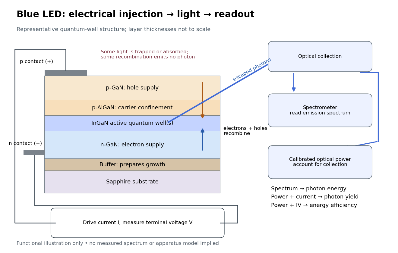
Blue light-emitting diode: carrier injection, emitting structure and optical readout
. Original functional schematic of a representative indium gallium nitride quantum well device on sapphire, not a reconstruction of the 1989 or 1994 devices. Layer thicknesses are schematic. Separate electrical and optical readings determine different properties: terminal electric potential difference and electric current, spectrum, and calibrated escaping optical power. The arrows represent routes through the device rather than a calculated energy band profile. Source. Details.