Three routes are donor doping, acceptor doping and above-gap illumination. All increase mobile carrier populations if the added states or excitations are effective rather than strongly trapped.
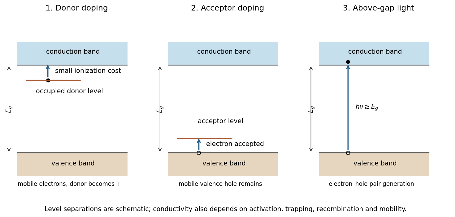
Original band diagrams for donor doping, acceptor doping and photogeneration in a gapped material
. Details. 
An appropriate donor impurity provides an occupied level just below the conduction band. Thermal ionization requires the smaller donor binding energy rather than the full host gap, supplying mobile electrons and n-type semiconductor behaviour. An appropriate acceptor impurity creates an available level just above the valence band; accepting a valence electron leaves a mobile hole, giving p-type semiconductor behaviour. Doping concentrations and compensation must permit useful carriers; an arbitrary impurity need not be an effective dopant.
For photoconductivity, absorbed photons with can excite valence electrons into the conduction band, producing electron–hole pairs. For the stated gap, the nominal threshold is about nm. Optical selection rules and absorption strength can shift the practical onset. The conductivity increase persists only while generation maintains carriers against recombination and trapping; it is not necessarily a permanent change to the material.
In each case, connects increased carrier density to conductivity. Defect-induced reductions in mobility can offset some of the gain, so the diagrams specify mechanisms rather than guarantee a numerical improvement for an unspecified preparation.
Articles by others on the same topic
There are currently no matching articles.