Finite-well confinement in a semiconductor heterostructure
ID: finite-well-confinement-in-a-semiconductor-heterostructure

Consider an original one-dimensional effective mass model with for and outside. Take the same positive effective mass everywhere, an abrupt interface, and no interactions. The wavefunction represents a transverse envelope; free motion parallel to the layer is outside this calculation. A double heterostructure laser need not be thin enough for this quantization to dominate its operation.
Set , , , and . The time-independent Schrödinger equation becomesHere denotes the dimensionless potential; a bound state has . Matching the wavefunction and its derivative at givesFor the even bound state, the interior solution is and the exterior solution is . For the odd bound state, replace by and by . The physical wavefunction is .
Wavefunction normalization includes both exterior tails, not just the active layer. Direct integration givesThe first two terms are the interior integral; the last is the total exterior integral. Thus the interior probability is , with the upper sign for even parity.
Choose . There is one even root in and one odd root in ; higher branches start beyond . Each left-hand side increases on its stated interval while decreases, proving uniqueness there. Numerically,These are calculated values of the chosen finite square well. The excited bound state lies closer to the barrier and has a longer exterior tail: being bound does not mean having unit probability inside the well.
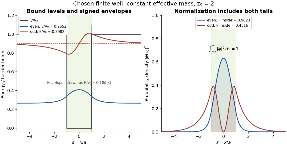

This model demonstrates electronic confinement, not optical refractive index confinement or a complete laser. Unequal effective masses, band bending, interface disorder and interactions require a more detailed model. In particular, continuity of the ordinary derivative above uses the chosen constant effective mass assumption.
New to topics? Read the docs here!