A direct band gap has its conduction band minimum and valence band maximum at the same crystal momentum. Near-edge absorption or emission can therefore conserve momentum with the electron and photon alone, since optical photon momentum is small on the Brillouin-zone scale. An indirect band gap has its extrema at different wavevectors and normally needs a phonon or another momentum-transfer process in addition to the photon.
Direct-gap materials are usually preferred for efficient light emission, because the radiative transition avoids the extra phonon-assisted process. Their stronger near-edge absorption also permits thinner photovoltaic absorbers. Indirect-gap materials can nevertheless make excellent solar cells: sufficiently thick optical paths, light trapping, long carrier lifetimes and suitable material quality can compensate for weaker absorption. The direct/indirect distinction alone does not rank every device.
This momentum distinction and the difference between bound exciton lines and the free-pair continuum are treated together in the primary effective-mass absorption theory.[ref]
Intensity of Optical Absorption by Excitons by Roger James Elliott. Abstract, direct versus phonon-assisted indirect transitions
Near the zone centre, . The tight-binding model becomesOnly appears at quadratic order, so the band effective mass tensor is isotropic. Higher-order lattice terms need not be isotropic.
For the conduction band, , so the curvature is positive andHere m and both beta parameters must be converted from eV to joules. The band edges at the zone centre areso the model has a direct gap . The mass values describe curvature at these extrema; they are not constant masses throughout the full tight-binding bands.
For the valence band, , so the electron curvature is negative. A missing electron is a positive-mass electron hole:The quadratic expansion has , so each diagonal electron inverse mass is . Reversing the sign to describe the missing electron gives the positive hole mass above. As in the conduction calculation, convert beta from eV to joules and use m; the result applies near the band edge.
The smaller gives the valence edge a larger density-of-states prefactor than the conduction edge. If the Fermi level were exactly halfway across the gap, there would therefore be more thermally generated holes than electrons. Charge neutrality in an intrinsic semiconductor requires equal carrier densities, so the chemical potential moves upward: it suppresses holes while increasing electrons.
Explicitly, in the nondegenerate limit,and gives the intrinsic Fermi levelSince , the Fermi level lies in the upper half of the gap at finite temperature.
The supplied inverse- density-of-states rule gives the correct ordering. Strictly, an isotropic three-dimensional parabolic band has a prefactor proportional to , rather than ; this changes the size of the displacement but not its sign. At zero temperature the limiting intrinsic expression approaches midgap; a chemical potential in a completely empty gap is not uniquely fixed by carrier neutrality alone.
Relative electron–hole motion uses the exciton reduced mass, rather than either band mass alone:In a screened hydrogenic Wannier-Mott exciton, replace by and by in the hydrogen binding-energy scale. ThereforeThe effective Rydberg is an energy here, not a spectroscopic inverse length. Its scale is reduced both by dielectric screening and by the small band reduced mass. The associated radius is about Å, several lattice spacings, consistent with using an extended-pair model as a first approximation rather than a tightly localized molecular exciton.
The Exciton Rydberg series lies below the unbound electron–hole threshold:Using eV and eV givesTheir positive exciton binding energies relative to the continuum are meV and meV, respectively.
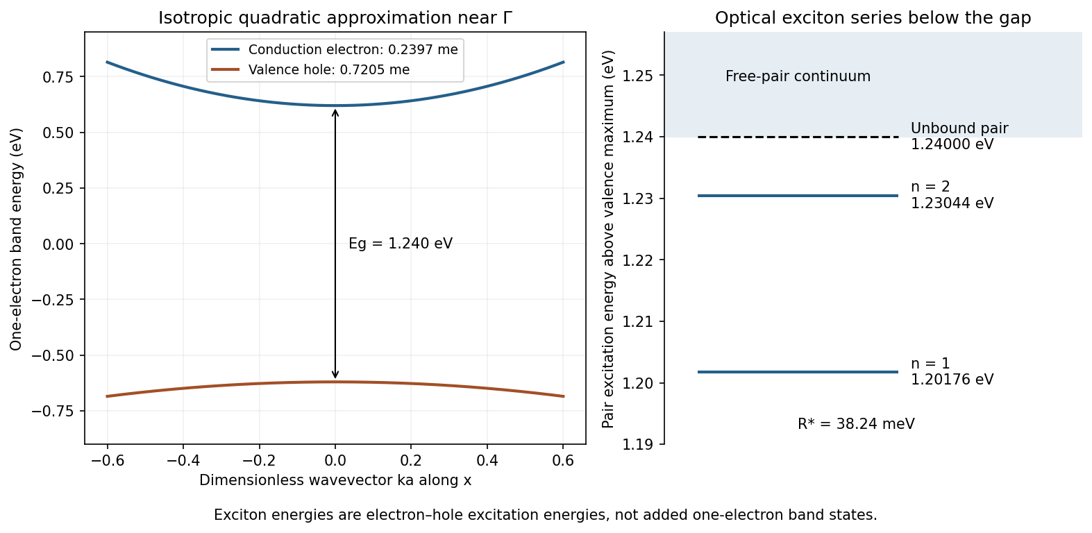
Original near-zone-centre band curvatures and hydrogenic exciton levels measured above the valence-band maximum
. Details. 
These are optical electron–hole excitation energies for negligible centre-of-mass momentum, not new occupied one-electron states inside the valence band. The simple model predicts their locations; observing a particular line also requires a nonzero optical transition matrix element and adequate linewidth.
At cryogenic temperatures, the intrinsic carrier concentration is exponentially small, while a low phonon population permits relatively sharp band-edge and exciton spectral features. Near room temperature, thermal electron–hole generation increases strongly:This generally raises intrinsic conductivity, although increased phonon scattering tends to lower the individual carrier mobilities. With a gap of eV, the material remains far from a degenerate metal at room temperature.
For optical structure, compare meV at 300 K with the exciton binding energies. The binding of meV is substantially smaller, so excited bound states are readily thermally disrupted and broadened. The ground binding of meV is larger but only about : the ground exciton need not disappear completely, yet strong thermal ionization and broadening can weaken its sharp line. A comparison with is a useful scale argument, not an exact bound-pair fraction independent of density or lifetime.
Thermal lattice expansion and electron–phonon interactions can also shift a real material's gap and optical edge. The given fixed tight-binding parameters contain no temperature dependence, so they do not determine the magnitude or even a universal sign of that extra gap shift. Within the stated model, the dependable trends are more thermally generated carriers and less distinct excitonic structure on warming.
Articles by others on the same topic
There are currently no matching articles.