Gate control of graphene carrier density
ID: gate-control-of-graphene-carrier-density

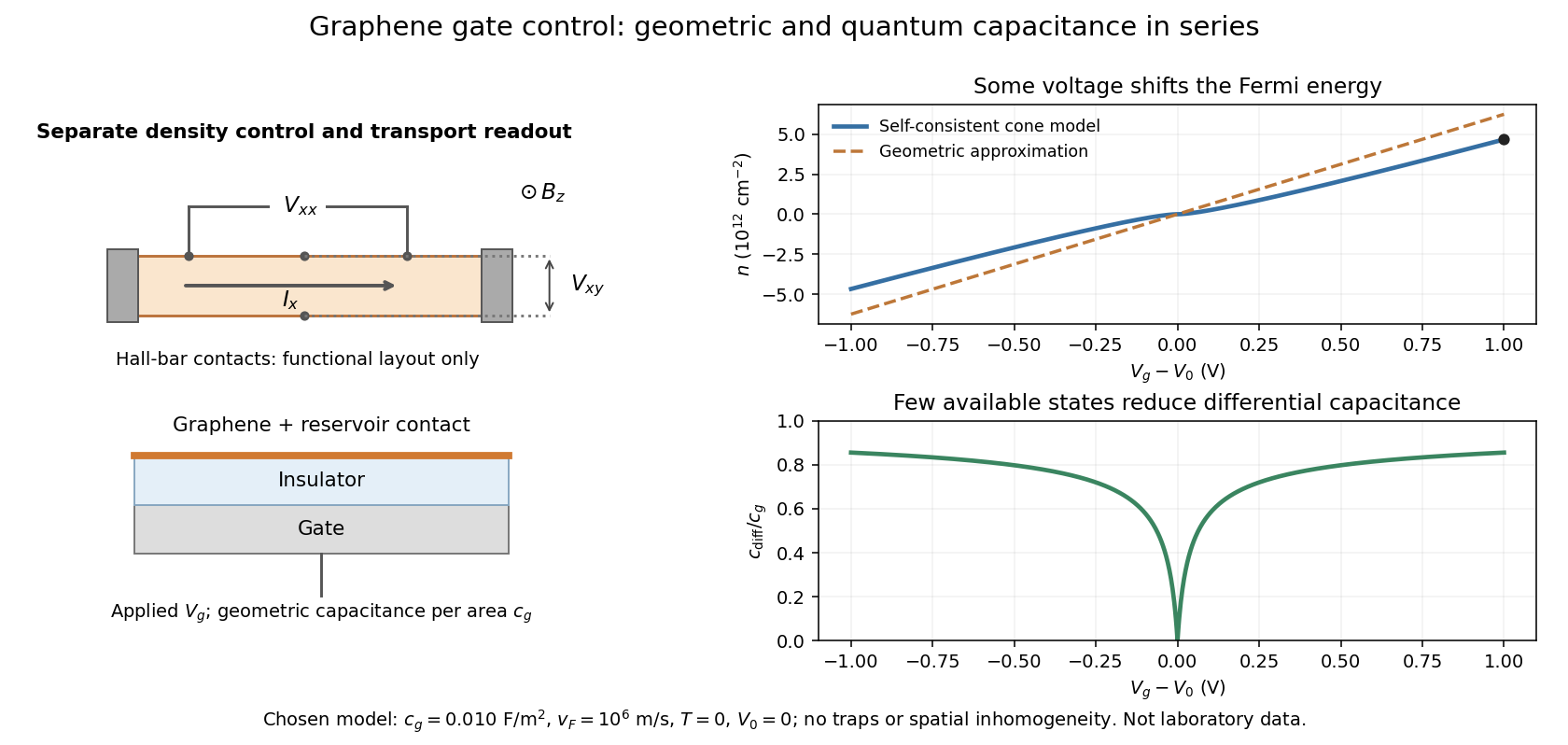
Consider an ideal uniform graphene sheet connected to an Electron reservoir, with an insulated gate. Let be geometric capacitance per unit area, the elementary charge, and the neutral-point offset. Neglect temperature, trapped electric charge and spatial inhomogeneity. A change in gate voltage pays for both the electrostatic potential drop, , and the change in the sheet's Fermi energy, . Here is measured relative to the band crossing; it is negative for excess electron holes.
Combine this relation with the carrier density in a graphene cone. Write , measured in volts, , and . ThenThe positive root is unique because is strictly increasing for . The often useful geometric approximation neglects the Fermi energy term. It overestimates in this model, especially near neutrality where relatively few states are available.
For a deliberately chosen model with , , and , the formulas give and . The purely geometric value would be . These are chosen-model predictions, not measurements of the historical devices. Numerical conversion uses the exact Planck constant and elementary charge.[ref]
Fundamental Physical Constants — Complete Listing by National Institute of Standards and Technology and others. Exact h and e entries; material parameters in this example are stipulated

New to topics? Read the docs here!