Graphene is a single layer of carbon chemical atoms arranged in a honeycomb lattice. A nearby gate can select predominantly Electron or electron hole conduction, as demonstrated by the graphene exfoliation and field-effect experiments.[ref]
Electric Field Effect in Atomically Thin Carbon Films by Konstantin Novoselov and others. pp.1–2, mechanically cleaved films, gate and Hall response
A useful question is how geometry changes motion. The nearest-neighbour model of graphene starts with three equivalent bonds from each site and two sites per primitive cell. Interference between those three hopping paths makes two energy bands meet; near their meeting, energy grows linearly with distance in wave vector. The resulting Dirac cones explain why an atomic sheet can imitate one aspect of a relativistic particle while remaining an ordinary material with contacts, defects and boundaries.
Take a planar honeycomb lattice with two sites per primitive cell and one localized atomic orbital per site. In this explicitly idealized tight-binding model, all three nearest-neighbour hopping matrix elements are , with ; there is no on-site offset or further-neighbour hopping. Ignore Electron interactions and treat physical spin as a separate degeneracy. Let the bond length be , and choose the three vectors from an site to its neighbours asThe Bloch state amplitudes on form a two-component vector. A consistent phase convention gives the HamiltonianIts characteristic equation is , giving the two displayed energy bands. The two-component structure comes from the two sites, rather than two values of physical spin. This is a particularly small matrix model in which a crystal's geometry creates an unexpected low-energy law.
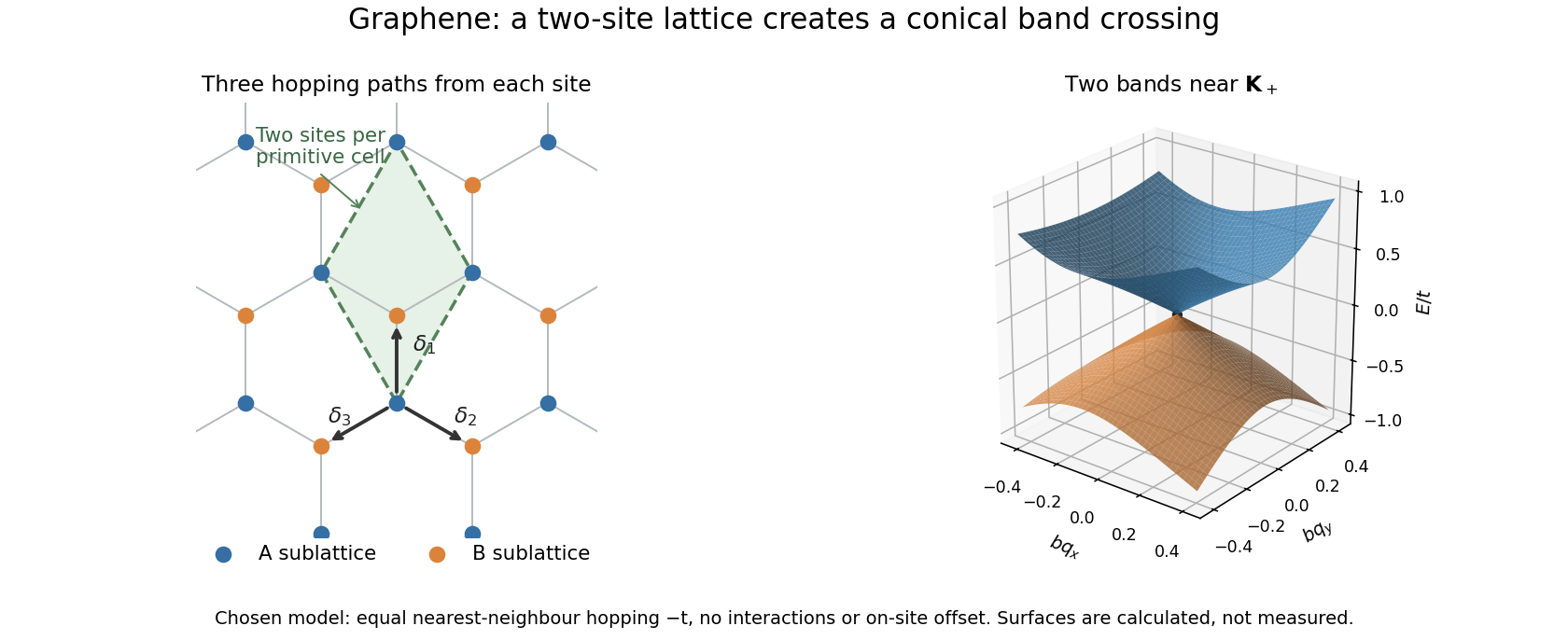
A honeycomb lattice produces two touching electronic bands
. Original nearest-neighbour model with the defined bond vectors. The surface shows the calculated bands near one zero of , with distance in units of inverse bond length and energy in units of the hopping magnitude. These are model energies, not measured band data. Source. Details.Historically, Philip Russell Wallace used a tight-binding model to investigate the electronic band structure of graphite in 1947. The material in that paper was layered graphite; the single-sheet model here isolates one simpler part of the problem.[ref]
The Band Theory of Graphite by Philip Russell Wallace. Publisher abstract: tight-binding bands and Brillouin zones of graphite; published 1 May 1947
At either displayed wave vector, the three complex hopping amplitudes add to zero: . Therefore the energy bands touch. There are two inequivalent electronic valleys; other equivalent corners are related by reciprocal-lattice translations. Setting and retaining first-order terms giveswhere are Pauli matrices. For example, at , . The matrix has the form of a massless two-dimensional Dirac Hamiltonian. Here is a material-model velocity, rather than the vacuum speed of light; this description does not change an Electron's vacuum rest mass. It describes the dispersion relation of electronic excitations near a band crossing.
At and positive energy, a normalized eigenvector for is . Its Pauli matrix expectation values give the displayed direction. This pseudospin records the relative amplitudes and phase on the two sublattices. Real spin supplies another label; confusing these two labels would double-count states and misinterpret the two-band Hamiltonian.
Assume zero temperature, the linear Dirac cone, and both real-spin states and both electronic valleys. Define as excess Electron number per unit area, negative for an excess of electron holes, relative to neutrality. A filled circular region of radius in wave vector space containsThus the excess carrier density grows quadratically with the Fermi energy, unlike the constant density of states of a parabolic two-dimensional band. Differentiating gives the positive density of states per unit area, . Both the geometry of occupied states and the fourfold degeneracy matter to the coefficient.
A massless-cone description permits a nonzero cyclotron effective mass. For a circular constant-energy contour of area , the semiclassical definition givesThe vanishing mass parameter in a Dirac Hamiltonian and the finite cyclotron response away from neutrality are different statements. This makes the temperature dependence of Shubnikov-de Haas oscillations a useful test of the dispersion rather than a measurement of an Electron's vacuum rest mass.
Andre Geim, Konstantin Novoselov and collaborators mechanically cleaved graphite, identified thin flakes, and fabricated multi-terminal Hall bars on oxidized silicon. A substrate gate changed the carrier density; longitudinal electrical resistance and the Hall coefficient supplied different checks. The 2004 report included one-, two- and three-layer devices and described a few-layer semimetal interpretation. Layer identification and electrical control were separate experimental achievements.[ref]
Electric Field Effect in Atomically Thin Carbon Films by Konstantin Novoselov and others. pp.1–2 and Figs.1–2: preparation, thickness selection and electrical measurements
The 2005 monolayer study used an optical microscope, electron microscopy and atomic force microscopy to select monolayers. It then measured Shubnikov-de Haas oscillations as temperature, gate voltage and magnetic field varied. Their damping inferred a density-dependent cyclotron effective mass; comparison with oscillation frequency tested a linear dispersion relation. A comparison with two-layer devices also distinguished their quantum Hall effect sequences. These are complementary tests of the monolayer model, rather than consequences of finding a thin-looking flake alone.[ref]
Two-Dimensional Gas of Massless Dirac Fermions in Graphene by Konstantin Novoselov and others. pp.1–3, Figs.2–4: monolayer selection, oscillation damping and bilayer comparison
Consider an ideal uniform graphene sheet connected to an Electron reservoir, with an insulated gate. Let be geometric capacitance per unit area, the elementary charge, and the neutral-point offset. Neglect temperature, trapped electric charge and spatial inhomogeneity. A change in gate voltage pays for both the electrostatic potential drop, , and the change in the sheet's Fermi energy, . Here is measured relative to the band crossing; it is negative for excess electron holes.
Combine this relation with the carrier density in a graphene cone. Write , measured in volts, , and . ThenThe positive root is unique because is strictly increasing for . The often useful geometric approximation neglects the Fermi energy term. It overestimates in this model, especially near neutrality where relatively few states are available.
For a deliberately chosen model with , , and , the formulas give and . The purely geometric value would be . These are chosen-model predictions, not measurements of the historical devices. Numerical conversion uses the exact Planck constant and elementary charge.[ref]
Fundamental Physical Constants — Complete Listing by National Institute of Standards and Technology and others. Exact h and e entries; material parameters in this example are stipulated
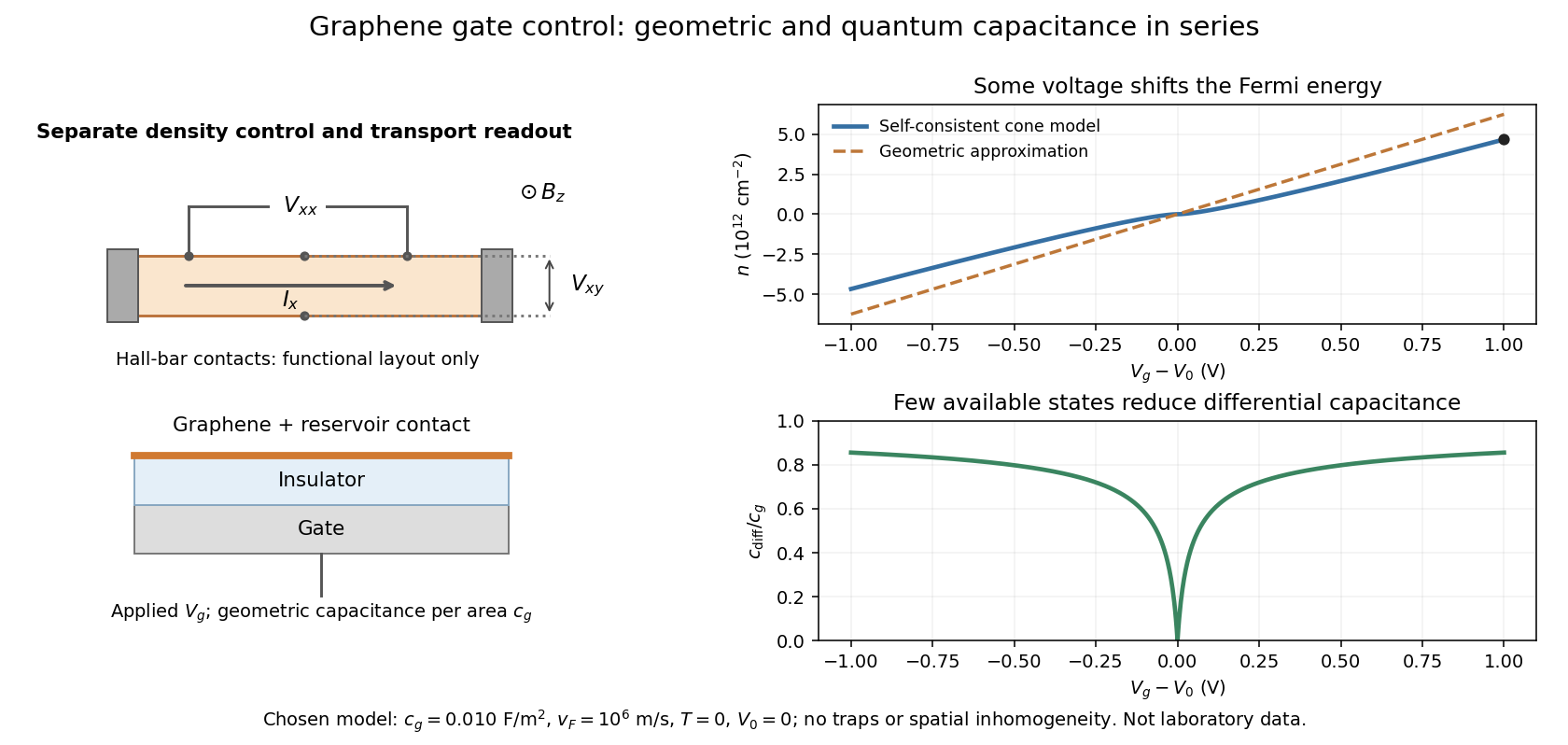
The quantum capacitance per unit area is . Differentiating the gate equation givesThus the available electronic states act as a second contribution in series with geometric capacitance. At exact neutrality the ideal zero-temperature model has ; actual finite-temperature or spatially nonuniform samples need a broader description. A capacitance measurement can therefore probe the density of states, rather than geometry alone.
Articles by others on the same topic
Graphene is a single layer of carbon atoms arranged in a two-dimensional honeycomb lattice. It is known for its remarkable electrical, thermal, and mechanical properties. Here are some key characteristics and applications of graphene: ### Properties: 1. **Strength**: Graphene is extremely strong—about 200 times stronger than steel—yet very lightweight. 2. **Electrical Conductivity**: It has exceptional electrical conductivity, making it conducive for electronic applications.