Arsenic has five valence electrons, whereas silicon has four. A substitutional arsenic atom can therefore supply an extra electron after participating in the silicon bonding network. It acts as a shallow donor impurity, introducing a localized level just below the conduction band. Ionizing that donor costs much less energy than excitation across the full band gap.
At the lowest temperatures, donor electrons remain bound and the valence band is filled. Mobile-carrier populations are negligible: this is dopant freeze-out. Initial heating releases donor electrons into the conduction band, producing a rapid rise in conductivity governed by the shallow-donor energy scale. The positive ionized donor charge compensates the released electronic charge; the bulk need not acquire net charge.
At intermediate temperatures, nearly all donors are ionized but intrinsic electron–hole generation is still small. In an uncompensated sample,where is donor number density. The supply of donor electrons is finite, so further heating cannot keep creating them. This is the extrinsic plateau under the approximation of weakly varying mobility, and its carrier density is much larger than that of the undoped sample at the same temperature. In real material, scattering changes mobility, so donor exhaustion alone predicts a carrier-density plateau rather than guaranteeing perfectly flat conductivity.
At higher temperatures, intrinsic generation becomes comparable to and then exceeds the donor contribution. Once , the populations approach , and activation across the main gap causes the steeper rise. The relevant regimes are therefore freeze-out, donor exhaustion, and intrinsic excitation, not three successive types of dopant.
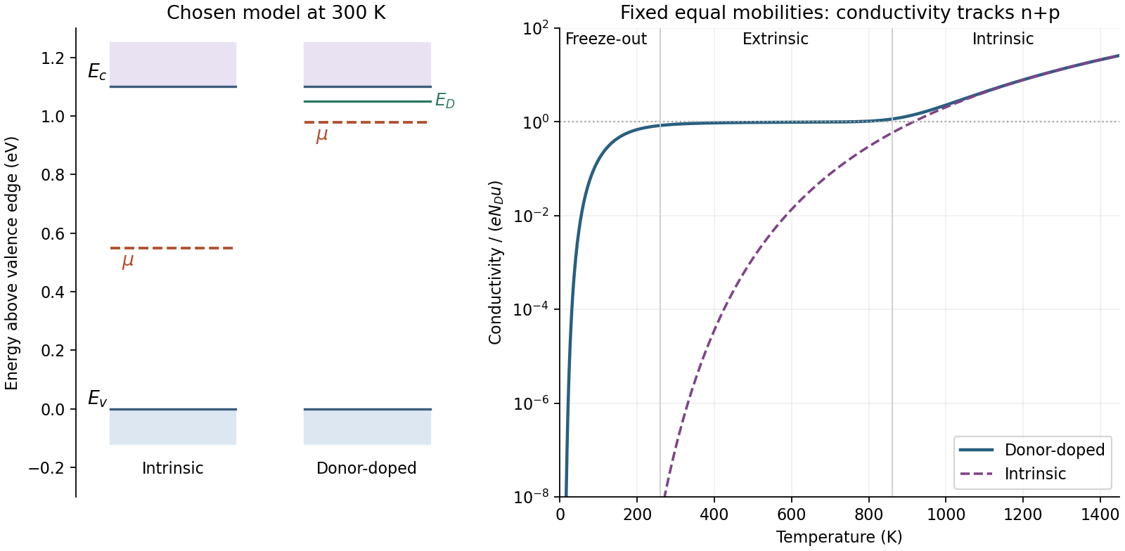
Donor occupation, Fermi-level position and three conductivity regimes
. Original illustrative model, not measurements of arsenic-doped silicon. The right panel solves charge neutrality with partial donor ionization and intrinsic carriers, assuming fixed equal electron and hole mobilities. Chosen parameters are , donor binding and . The left panel illustrates the resulting room-temperature energy ordering, including a Fermi level below the donor level. Details.
The ambient-temperature Fermi level is raised into the upper part of the gap, toward the conduction-band edge, relative to intrinsic silicon. The sample is an n-type semiconductor: ionized donors supply many more conduction electrons than the intrinsic population.
For a nondegenerate, substantially ionized sample with negligible acceptors, . With effective density of states , the conduction-band relation givesBecause a few ppm normally gives at ambient temperature, the chemical potential remains below the conduction-band edge rather than entering it as in a strongly degenerate semiconductor. Its precise position requires the dopant density, density of states and degree of ionization; the broad qualitative shift is fixed by donor doping.
It is not necessary for to lie between the donor level and the conduction edge. In a substantially ionized nondegenerate sample, the chemical potential can lie below the shallow donor level, as in the illustrative diagram. Donor ionization is determined by the level's occupation relative to ; a finite-temperature Fermi level is not the highest filled one-electron level of every individual configuration.
Articles by others on the same topic
There are currently no matching articles.