One suitable platform is a monolayer molybdenum disulfide semiconductor. An electrostatic accumulation gate supplies conduction electrons whose motion is confined to the atomic sheet; source and drain contacts act as reservoirs. A clean insulating substrate and dielectric or encapsulation reduce disorder and prevent gate leakage. Two split gates deplete the adjacent sheet and leave a narrow conducting gap, thereby confining the in-plane transverse direction while retaining transport along the gap.
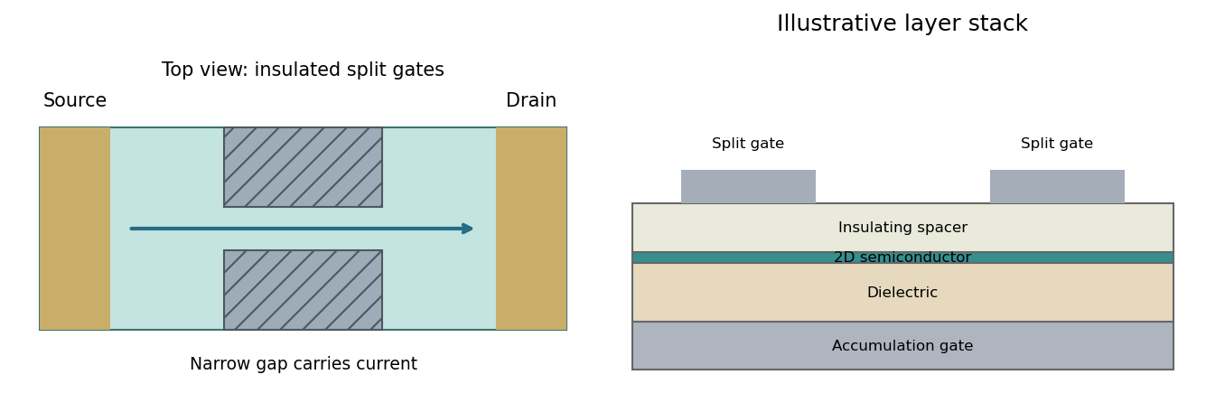

Apply a small source-drain voltage, measure the current and determine linear-response conductance while tuning the split-gate voltage and carrier density. A graphene sheet is another two-dimensional carrier system, but its lack of an ordinary gap complicates purely electrostatic confinement; etched boundaries or a suitable gapped architecture may be needed. A two-dimensional material does not by itself guarantee ballistic transport or resolved subbands.[ref]
Split-gated point-contact in MoS2-hBN structures by Chithra H. Sharma and Madhu Thalakulam. Electrostatic confinement in a two-dimensional semiconductor platform
Articles by others on the same topic
There are currently no matching articles.