Let run along the wire and across it. In a separable approximation,Transverse confinement gives discrete levels , but the long unconfined direction has a nearly continuous longitudinal wave vector and a plane-wave factor. The result is a family of one-dimensional subbands, not a completely discrete spectrum in both in-plane directions. For a hard-wall width , ; an electrostatic confinement potential gives different thresholds. The suppressed out-of-plane degree of freedom is already frozen into the 2DEG subband.
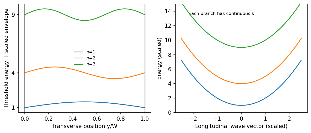
Discrete transverse thresholds coexist with continuous longitudinal dispersion
. Source. Details. One suitable platform is a monolayer molybdenum disulfide semiconductor. An electrostatic accumulation gate supplies conduction electrons whose motion is confined to the atomic sheet; source and drain contacts act as reservoirs. A clean insulating substrate and dielectric or encapsulation reduce disorder and prevent gate leakage. Two split gates deplete the adjacent sheet and leave a narrow conducting gap, thereby confining the in-plane transverse direction while retaining transport along the gap.
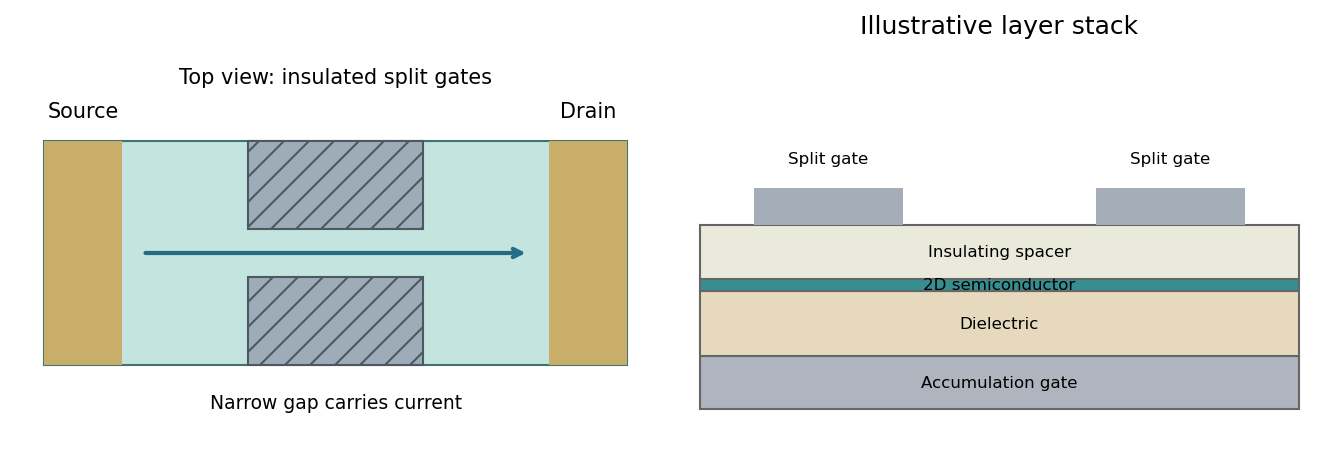
Apply a small source-drain voltage, measure the current and determine linear-response conductance while tuning the split-gate voltage and carrier density. A graphene sheet is another two-dimensional carrier system, but its lack of an ordinary gap complicates purely electrostatic confinement; etched boundaries or a suitable gapped architecture may be needed. A two-dimensional material does not by itself guarantee ballistic transport or resolved subbands.[ref]
Split-gated point-contact in MoS2-hBN structures by Chithra H. Sharma and Madhu Thalakulam. Electrostatic confinement in a two-dimensional semiconductor platform
For a clean, adiabatically connected GaAs channel at low temperature and small bias, opening successive spin-degenerate subbands givesConductance therefore shows a staircase of plateaux, rather than the continuously geometry-dependent classical Ohmic result. Each fully transmitted mode contributes approximately . More positive, or less negative, depletion-gate voltage opens a conventional GaAs constriction; more negative voltage closes it.
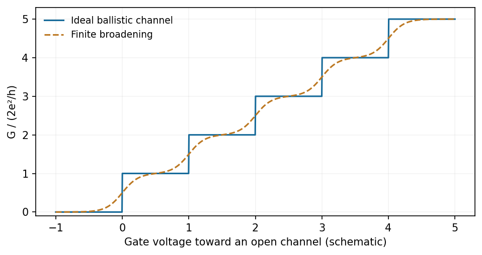


Require subband spacings larger than thermal and bias broadening and a mean free path exceeding the constriction length. The general Landauer formula is with each spin/valley channel counted separately. A material with additional valley degeneracy need not have the same step sequence as GaAs, and imperfect transmission or contact resistance blurs the ideal plateaux.
Articles by others on the same topic
There are currently no matching articles.