A semiconductor has an electronic band gap and a conductivity strongly affected by temperature, impurities and carrier injection. Optical absorption can create mobile electrons and holes, enabling a photodiode.
The useful feature of a semiconductor is that its charge carrier population can be controlled. Semiconductor doping changes the supply of mobile electrons or electron holes; carrier injection changes their population away from thermal equilibrium. A transistor turns that control into an electronic amplifier: a small input signal controls a larger flow of supplied energy.
For a uniform semiconductor in a weak electric field, a simple drift model writes its electrical conductivity asHere is the elementary charge, are the number densities of mobile electrons and electron holes, and their positive charge carrier mobilities. The two contributions add because opposite electric charges drift in opposite directions and therefore carry electric current in the same direction. This model assumes fixed temperature and mobilities and omits diffusion from density gradients.
An original dimensionless example isolates the effect of carrier injection. Suppose initially and . Adding equal excess populations gives , even though the added electron holes remain a minority carrier population. A semiconductor can respond strongly to a small injected population without changing its underlying band gap.
An extrinsic semiconductor has mobile electron and electron hole populations substantially controlled by electrically active impurities rather than solely by intrinsic thermal pair production. Donor impurities favor electron conduction and acceptor impurities favor hole conduction. Ionization, compensation and the temperature-dependent intrinsic population determine whether a given doped specimen is actually in its extrinsic transport regime.
Symmetry of the excitation spectrum under exchange of conduction band electrons and valence band holes, after choosing a central zero of energy. In a two-band model with equal effective masses and equal degeneracy factors, charge neutrality in an intrinsic semiconductor fixes the chemical potential at that central energy. Indeed the Fermi-Dirac distribution obeys , so excitation populations are equal at every positive energy.
A compound semiconductor built from group-III and group-V elements, such as gallium arsenide. Many common members have a zinc blende structure, while other materials or growth conditions give a wurtzite structure. The chemical family alone does not fix a direct rather than indirect gap or a particular band ordering.
A compound of aluminium and phosphorus, with two chemical atoms per primitive unit cell in its usual zinc blende structure. Its two inequivalent atomic basis sites give six phonon branches, three acoustic and three optical.
A common unstrained cubic III-V band ordering consists of an s-like conduction doublet, a p-like quartet and a lower spin-orbit split-off doublet. In the cubic limit the quartet gives heavy-hole and light-hole bands that meet at the Gamma point; different curvatures and direction-dependent mixing distinguish them away from it. The split-off valence band is separated by . This common ordering is a model to check against the actual material, not a consequence of chemical stoichiometry alone.
An organic solid supporting electronic charge transport; conjugation, intermolecular packing and disorder influence its properties.
Molecular excitations in organic semiconductors often retain strong local character. Weak screening supports Frenkel excitons or intermolecular charge-transfer admixtures, so a photon can create a bound neutral excitation rather than free carriers. Transition dipoles, spin selection rules, molecular packing and Franck-Condon factors set the bright spectral features. Disorder and thermal vibrations broaden them. Electronic overlap can also produce more delocalized excitons; the molecular limit is a useful model, not a definition covering every organic solid.
A soluble fullerene derivative, commonly the C60-based phenyl-C61-butyric acid methyl ester, used as an electron acceptor in organic photovoltaic blends. Different fullerene cage sizes give related derivatives.
A conjugated polymer with hexyl-substituted thiophene repeat units, often used as a model electron-donor semiconductor. Regioregularity and packing influence its optical and transport response.
Recombination of charge carriers through surface or interface states. Surface passivation and suitable wider-band-gap window or field layers can reduce minority-carrier losses in a photovoltaic device.
Reduction of electronically active surface states or of minority-carrier access to them. Chemical bond termination and electrostatic field effects can both suppress surface recombination.
A contact with approximately linear, nonrectifying current–voltage behavior and suitably low contact resistance in its operating range.
A pad-spacing method separating contact and sheet resistance. For uniform ohmic contacts, ; the transfer length is . A rectifying Schottky junction requires bias-dependent analysis.
An area-normalized interface resistance, in resistance times area. For nonlinear contacts specify the bias-dependent differential quantity.
An energy barrier at a metal–semiconductor contact. Depletion width and tunneling depend on doping; interface states can limit simple work-function predictions.
A carrier regime in which conduction electrons and valence holes are dilute enough to use Boltzmann approximations to Fermi-Dirac occupations. Typically and are required for both species.
An increase of electrical conductivity due to light-generated mobile carriers. Generation, recombination, trapping and mobility determine the observable response.
Indium arsenide, InAs, is a III-V semiconductor. An InAs island in a larger-gap host can provide quantum confinement for electrons and electron holes. The optical transition energy of a strained, confined island is not simply the bulk material's band gap.
A quantum dot confines electrons and electron holes in all three spatial directions, producing discrete energy levels. A semiconductor island surrounded by a larger-band gap material is one realization. Its optical excitation and electron-hole recombination depend on confinement, Coulomb interactions and electric-dipole selection rules.
A small electron island confined laterally by depletion gates in an already vertically confined two-dimensional electron gas. Tunnel barriers couple it to reservoirs, and a plunger gate tunes charge occupation. Coulomb blockade and orbital confinement resolve individual electron additions.
A single confined electron's two spin states form a qubit when initialization, coherent rotations and measurement are controlled. Local driving rotates one spin; gate-controlled exchange can entangle neighboring dot spins. Spin-to-charge conversion permits electrical readout. Observing charge blockade alone does not demonstrate coherent qubit operation.
Two capacitively and tunnel-coupled electron islands with separately tunable occupations. Detuning controls which dot holds an electron and whether two-electron charge states such as and are accessible.
A single electron shared by two dots has a left/right charge basis. In that basis, a two-level model is , where detuning sets the energy imbalance and tunnelling mixes the states. Electrical control and charge sensing are direct, but electric-potential fluctuations also couple strongly to the encoded information.
An effective coupling that separates the two-electron singlet state and triplet states by energy . For a symmetric two-site Hubbard model with weak tunnelling and charging cost , . Gate-controlled detuning and tunnelling change the interaction; the simple expression does not hold at arbitrary detuning or strong charge hybridization.
A measurement method in which spin-dependent tunnelling or allowed charge transfer maps a spin outcome onto a distinguishable dot charge state. Quantum-dot charge sensing then records that charge. The measurement axis or singlet/triplet observable must be specified.
Map states with unequal escape rates onto distinct charge outcomes after an interval between their characteristic escape times. Both removal energies can lie above the reservoir chemical potential, so their splitting need not be thermally resolved. A useful rate difference must have a physical origin: a demonstrated single-dot example uses a two-electron singlet state and triplet state with different occupied orbitals. A bare single-electron Zeeman pair in the same orbital does not automatically provide the required rate contrast.[ref]
For independent exponential escape, equal prior probabilities and no state relaxation, the mean classification error is . Setting its derivative to zero gives the displayed interval. The error increases both when the fast state is not given enough time to escape and when the slow state is given too much. Detector bandwidth, relaxation and reloading require an expanded measurement model.
Suppression of charge transfer by spin symmetry and the Pauli exclusion principle. For a double quantum dot, a singlet state can enter the lowest singlet, whereas a triplet state is blocked if the required triplet lies above the accessible energy window. Spin mixing or relaxation can lift blockade.
A resonantly driven local electron-spin rotation can give a blocked two-dot triplet a singlet component, allowing spin-conserving charge transfer to a lowest-orbital doubly occupied dot. A common rotation of two perfectly identical spins does not mix singlet and triplet sectors, so relative spin rotation or an additional mixing mechanism is essential. Leakage-current spectroscopy tests resonant lifting; pulse-duration oscillations add evidence for coherent control.
Place the reservoir chemical potential between the lower and higher Zeeman-split one-electron dot levels. The excited state can leave while the ground state remains trapped; a time-resolved charge sensor detects the temporary empty state. Thermal errors, missed fast tunnelling and relaxation before escape limit fidelity.
Detection of a dot's charge through its capacitive influence on a nearby quantum point contact or single-electron transistor. Discrete charge changes shift the sensor response, allowing individual tunnel events to be resolved even when direct current through the dot is too small to measure.
For a circular two-dimensional parabolic dot in perpendicular magnetic field, orbital levels are , with . The sign depends on the angular-momentum and signed-charge convention. At zero field the shell degeneracy is before spin; Zeeman and interaction terms require separate treatment.
A nanocrystal with one semiconducting composition surrounded by another. band offsets, interface quality and shell thickness govern carrier confinement and coupling to external traps. type-I band alignment favors electron and hole localization together; type-II band alignment can separate them. A larger shell band gap does not by itself determine those offsets.
The difference between successive electron-addition chemical potentials. In a constant interaction model it is , separating electrostatic charging from orbital level spacing. Spin, exchange and correlation can change the orbital contribution.
Filling a degenerate orbital shell produces a larger addition energy for the next electron. In a circular two-dimensional harmonic potential, shell has orbitals and capacity including spin. Cumulative closed-shell occupancies are . Charging and orbital contributions must be separated, and anisotropy or exchange can split the ideal shells.
A quantum dot of InAs embedded in gallium arsenide confines injected electrons and electron holes. Strain-driven island formation supplies dots with lateral dimensions of order tens of nanometres and heights of a few nanometres. In an electrically driven implementation, a dot lies in a junction's intrinsic region. Selecting one dot spatially and one radiative line spectrally turns discrete exciton recombination into a single-photon source. Pulsed injection must avoid re-excitation during the same collection window.
The pioneering electrically driven device used an areal dot density around , a GaAs p-i-n structure and an aperture selecting individual-dot light.[ref]
The effective density of states of a parabolic semiconductor band is its density of states integrated against a thermal Boltzmann factor measured from its edge. For one spin-degenerate valley,These quantities have units of number per volume, unlike the energy-resolved density of states. In a nondegenerate semiconductor, and ; multiple equivalent valleys add their contributions.
A scalar effective mass chosen to reproduce carrier state counting near a band edge. For equivalent ellipsoidal conduction valleys, when the displayed factor two accounts for spin degeneracy. The valley degeneracy is then already included and must not be multiplied in again. A conductivity mass weights inverse curvatures and is generally different; for an isotropically averaged set of ellipsoids, .
An intrinsic semiconductor has equilibrium mobile electron and electron hole densities set predominantly by thermal excitation across its band gap, rather than by semiconductor doping. In the nondegenerate regime, charge neutrality gives .
In a symmetric model with constant density of states per volume and energy in two broad bands, charge neutrality gives and . In the nondegenerate limit, . Thus the leading exponential activation law can coexist with an algebraic temperature prefactor.
For symmetric touching parabolic dispersions with constant density of states per energy band, including spin degeneracy, charge neutrality fixes . The Fermi-Dirac distribution gives and the thermal internal energy, including electrons and holes, is . Thus . Its large ratio to is compatible with the equipartition theorem because this excitation count grows with temperature and the heat capacity includes both species.
The chemical potential fixed by equal conduction-electron and valence-hole densities in an intrinsic semiconductor. In the nondegenerate parabolic-band model, .
For nondegenerate conduction bands and valence bands, charge neutrality gives . Taking logarithms yieldsFor single spin-degenerate parabolic extrema this becomes . Valley multiplicities or additional hole bands belong in and change the logarithm. The intrinsic chemical potential lies exactly at midgap only when the two effective density of states values agree.
For nondegenerate bands separated by , the intrinsic carrier concentration is , using the effective density of states . For fixed parabolic band effective masses and fixed gap, .
In a nondegenerate parabolic-band semiconductor with fixed density-of-states mass, , where . ThusA single measured value of does not determine its temperature dependence. A fixed-gap intrinsic model instead has , with the two effective density of states factors in . Identifying a crossover by gives an order-of-magnitude dopant-density estimate once that activation law is specified. At exact charge neutrality with , the total mobile-electron density is , so a crossover is not a sharp equality of every density definition.
For fixed band effective masses and band gap , the intrinsic carrier concentration obeys . ThusA base-ten plot against instead has slope after the prefactor correction. The intrinsic branch must be used, rather than the extrinsic plateau or dopant freeze-out branch. A changing gap or effective mass makes this an activation-energy estimate, and a small gap uncertainty can produce a much larger multiplicative uncertainty in a room-temperature minority density.
In thermal equilibrium, nondegenerate conduction electrons and valence electron holes share one chemical potential. Multiplying by cancels that chemical potential:This relation remains valid with semiconductor doping under the stated assumptions. Equality of the two individual densities, , additionally requires the intrinsic neutral case. Separate electron and hole quasi-Fermi levels in nonequilibrium need not obey this equilibrium product.
With one parabolic valley and two spin states at each band edge, the prefactor multiplying in the product is . Both populations must be nondegenerate; the Pauli reduction of the pinned-edge mass-action product quantifies a failure of the classical approximation.
For chemical potential at the conduction edge, divide the exact product by the classical prediction. The ratio is , where . It is less than one, approaches as , and approaches its square in the formal high-temperature parabolic model.
A homojunction joins regions of the same semiconductor material with different semiconductor doping. Its bulk band gap is the same on both sides. This distinguishes the electrostatic band bending of a simple equilibrium p-n junction from the material-dependent band offsets possible in a heterojunction.
A semiconductor with a comparatively large band gap; short-wavelength light-emitting diodes require sufficiently energetic optical transitions.
Electron-hole recombination that does not emit a photon; it competes with the radiative channel in a light-emitting diode.
Trap-assisted recombination through defect states that capture electrons and holes sequentially. It can occur in the bulk or near interfaces.
A localized electronic defect can capture a conduction electron and subsequently an electron hole, or the reverse sequence, returning to its original charge state. Energy is transferred to the lattice rather than an emitted photon. The two-step process can remove an electron-hole pair even when direct band-to-band photon emission is inefficient. Its rate depends on trap density, occupation and both capture rates; a single trapping event is not necessarily completed recombination.
An impurity that can accept an electron from the valence band, leaving a mobile hole. A shallow acceptor creates an impurity level in a crystal near and above the valence-band edge. Donor and acceptor levels are descriptions of appropriate dopants, not universal features of every impurity species.
A shallow acceptor can bind an electron hole through the screened Coulomb potential of a negatively charged impurity. A scalar band effective mass approximation gives a hydrogen-like bound-state ladder. Actual valence-band degeneracy and anisotropy can split levels and limit that approximation.
In gallium nitride, incorporated hydrogen can neutralize magnesium acceptor impurities. Activation treatments restore electrical activity; adding magnesium alone does not establish a mobile electron hole population.
An impurity that can supply an electron to the conduction band. A shallow donor has a localized occupied impurity level in a crystal near and below the conduction-band edge; thermal or other ionization releases its electron. The binding energy depends on the host dielectric response and effective mass.
Let an isolated donor impurity admit an empty ionized state with statistical weight and a singly occupied neutral state with statistical weight , with double occupation excluded. Its grand canonical ensemble weights are and , so multiplies the occupied-to-empty ratio. A nondegenerate empty state and two allowed electron spin orientations give ; a simplified single-state occupation model uses . With negligible electron holes and uncompensated donor impurities, charge neutrality and nondegenerate conduction occupation imply , where is the donor binding energy and the effective density of states.
A nondegenerate donor-bound state of energy zero and an excited representative conduction level of energy and degeneracy have the displayed bound probability by canonical state counting. The inferred degeneracy from one measurement is . At finite fixed , the probability decreases from1 toward as temperature grows. A temperature-independent effective degeneracy is an assumed two-level approximation; a full conduction-band density of states can behave differently.
In a scalar effective-mass dielectric model, the donor radius is . The effective mass reduces the kinetic-energy scale and dielectric screening weakens attraction. The corresponding binding energy scales as times the vacuum hydrogen binding energy.
For shallow hydrogenic donor states of radius and random donor number density , the mean spacing is of order . Taking this spacing comparable to gives ; a geometric diameter criterion instead gives . The orbitals have exponentially decaying tails rather than hard boundaries, so there is no exact geometric onset. Appreciable overlap also limits the independent-donor ionisation model; a genuine transport transition needs additional electronic physics.
A shallow donor impurity in an isotropic semiconductor can be approximated by an electron of effective mass in a Coulomb potential screened by relative permittivity . Its ground-state binding energy and radius areThe donor level lies below the conduction band. These are magnitudes: the bound electron's energy relative to the band edge is negative. Band anisotropy, short-distance impurity structure and screening by mobile carriers can invalidate the simple Bohr model rescaling.
An electron confined to a plane in the screened Coulomb potential , , has the radial ground state . The planar radial Laplacian is . Cancelling the term in the Schrödinger equation gives and . The binding magnitude is four times the three-dimensional effective Rydberg. Normalization in the plane gives . The ordinary three-dimensional electric field is retained; a logarithmic two-dimensional interaction is a different problem.
Mercury cadmium telluride is a semiconductor whose composition tunes its band gap and hence its long-wavelength absorption cutoff. It is widely used as the absorbing material in infrared detector arrays.
A p-n junction joins regions of a semiconductor with opposite majority charge carriers: electrons on one side and electron holes on the other. It provides the junction modeled by the Shockley diode equation.
Near an unbiased p-n junction, diffusion leaves exposed ionized donor impurities and acceptor impurities. Their electric field opposes further majority-carrier transfer. At thermal equilibrium, drift and diffusion balance; there is no net electric current. Forward bias reduces the barrier to carrier injection; reverse bias enlarges it. A heavily doped tunnel diode adds a different transport route, quantum tunnelling, that the ordinary Shockley diode equation omits.
A linearly graded p-n junction has net ionized doping near the metallurgical junction. In the depletion approximation, . With vanishing external field, neutrality places the depletion edges at and integration of Poisson equation givesThe field points from n to p and has largest magnitude at . The potential is cubic inside the layer.
For a linearly graded p-n junction, the signed p-side depletion charge per area is . Differentiating with respect to positive p-side voltage , using the linearly graded junction depletion width, gives the positive differential junction capacitance per areaThus is linear in . If stored charge denotes the positive n-side magnitude , its derivative with respect to is negative; the positive capacitance is instead for reverse-voltage magnitude . Neither definition uses the zero net charge of the whole depletion layer.
Integrating the electric field across a linearly graded p-n junction gives , where positive means forward bias. Thus the depletion region width depends on the cube root of the remaining barrier voltage. Both the space-charge density and integration range grow with width; this differs from the square-root width law of an abrupt uniformly doped junction.
The built-in potential of a p-n junction is the electrostatic potential difference established when carrier diffusion exposes ionized dopants until the opposing drift and diffusion currents balance. The equilibrium electrochemical potential is constant even though the electric potential and band edges vary. In a nondegenerate homojunction with neutral-edge majority densities , . This is band bending within the same material, not necessarily a discontinuous offset of different materials' band edges.
A tunnel diode is a p-n junction with sufficiently heavy semiconductor doping on both sides to make a thin depletion region and permit substantial interband tunnelling. The neutral regions are degenerate semiconductors. Its distinctive forward current-voltage characteristic contains a peak followed by a valley: over part of the curve, increasing the applied electric potential difference decreases the electric current. The Esaki tunnel-diode experiment made this behavior experimentally concrete.
The useful quantity is the local slope, not the ratio of total voltage to total electric current. With conventional electric current entering the positive-voltage terminal, defineNegative differential resistance means , hence where defined. A forward operating point can still have , and absorbed power . A small voltage increase then gives a negative current increment; this does not make the total electric current negative or turn the device into an unlimited source of energy. The external supply sets the operating point and supplies the energy available for an electronic amplifier.
An original idealized construction explains the shape. Put the n-type semiconductor on the left and the p-type semiconductor on the right. Take as the elementary charge and . Increasing forward bias lowers the right-hand electron energy levels relative to the left. Denote the two reservoir electrochemical potentials by , so that . At zero temperature, occupied left-hand conduction band states extend up to ; empty right-hand valence band states start at . For transfer conserving electron energy, the available interval isIt is nonempty only when its upper endpoint exceeds its lower endpoint. Both an occupied initial quantum state and an empty final quantum state must exist at the same energy. The Pauli exclusion principle prevents transfer into an already occupied final quantum state.
For the original diagram, choose arbitrary energy units with , , and , where is in those units. The available interval has widthThus , , , and . Initially forward bias opens a transfer window; further forward bias closes it by moving the right-hand valence band edge below the left-hand conduction band edge. This is a state-counting illustration, not a formula for a measured electric current.
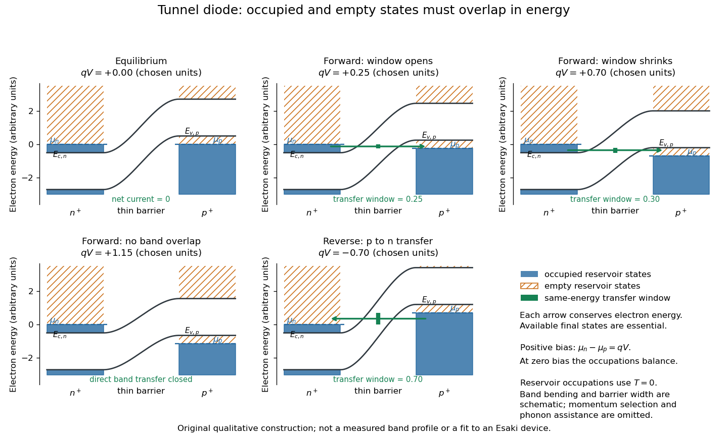
Tunnel diode: energy band alignment and occupied-to-empty state overlap
. Original chosen energy band construction, with n-type semiconductor on the left and p-type semiconductor on the right. Blue shading denotes occupied reservoir states; orange hatching denotes empty reservoir states. Green arrows mark equal-energy transfer. The central barrier and band bending are schematic; all energies are arbitrary, and the drawing is not an experimental image or measured band profile. Source. Details.For reverse bias, the transfer direction changes: occupied right-hand valence band states can feed empty left-hand conduction band states. In the same construction, opens the interval for this reverse transfer. A narrow depletion region allows a large reverse quantum tunnelling electric current at small electric potential difference, whereas the ordinary Shockley diode equation predicts only a small reverse saturation electric current before diode reverse breakdown. At zero biasing, equal reservoir occupations give zero net electric current; quantum tunnelling does not require a net equilibrium flow.
A finite-temperature refinement replaces sharp occupation cutoffs with the Fermi-Dirac distribution. An illustrative weak-transfer expression isHere describes allowed initial/final quantum states and their coupling, and are Fermi-Dirac distributions with the respective electrochemical potentials. The occupation difference follows by subtracting the reverse transfer factor from the forward one: . An overlap interval alone does not determine : transmission probability, density of states, crystal momentum selection and phonons can matter. A complete germanium calculation is more demanding than multiplying two constant density of states factors. At larger forward bias, ordinary carrier injection and diffusion supply a rising current branch even after direct band overlap is lost.
Leo Esaki's 1958 report describes alloy-fabricated germanium p-n junctions, with acceptor impurity concentration and donor impurity concentration approximately . Its readout was the current-voltage characteristic: a forward peak occurred at . The report says specimens could be reproduced; above the forward branch approximately followed the ordinary Shockley diode equation.[ref]
New Phenomenon in Narrow Germanium p-n Junctions by Leo Esaki. New Phenomenon in Narrow Germanium p-n Junctions, p. 603, opening paragraph and Fig. 1; opening reproduced on slide 2 of the Trinity College Dublin lecture PDF
In his 1973 lecture, Leo Esaki recalls an earlier junction whose strong room-temperature reverse conduction preceded a negative-slope forward segment revealed by cooling. Its estimated zero-bias width was about ångströms (), supported by capacitance measurements. Increasing semiconductor doping further made the negative slope visible across the measured temperatures, including room temperature. Thus preparation and temperature variation were experimental controls, not merely changes to a theoretical diagram. The low onset voltage argued against avalanche production of electrons and electron holes; the energy band explanation connected the forward decline to loss of available final states.[ref]
Long Journey into Tunneling by Leo Esaki. Long Journey into Tunneling, section II, printed pp. 120–122, Figs. 3–5; inspected institutional mirror at kapitza.ras.ru
The historical readouts were junction electric current versus applied electric potential difference and a separate capacitance check; preparation and temperature were varied. The cited descriptions do not identify a meter model or give a complete wiring diagram.
For a modern repetition, measure junction voltage directly while stepping the supply and recording electric current, repeat both sweep directions, and compare temperatures and differently doped specimens. These are proposed controls, not a reconstruction of the historical apparatus. Lead electrical resistance, Joule heating, contact quality and voltage resolution can obscure the result. The tunnel-diode load-line stability calculation also predicts that an external resistor can make a negative-slope operating point inaccessible in a slow sweep. A jump in terminal readings then need not mean the underlying current-voltage characteristic is discontinuous.
A current-voltage characteristic determines possible steady operating points; it does not alone determine their linear stability. Consider an ideal voltage source feeding a tunnel diode through a resistor , with a positive constant capacitance across the junction. Assume a quasistatic device relation and neglect inductance, transit delays, noise and heating. Kirchhoff's current law gives the original one-state modelA steady operating point satisfies : the device curve intersects the descending supply line. This is the source-side counterpart of a resistive load line. A small perturbation obeysThus the equilibrium point is locally attracting if and unstable if the inequality reverses. Equality requires higher-order analysis. Even on a negative differential resistance segment, a sufficiently small supply electrical resistance can stabilize this model. The assumption about the electrical circuit matters: an inductive or delayed circuit has additional state variables and may behave differently.
Choose an original toy forward characteristic, with no fitted device parameters:where , and . For every , , so this entire forward curve absorbs positive total power. NeverthelessThe model therefore separates negative differential resistance from negative total . The corresponding peak and valley are at approximately and ; these voltages deliberately differ from the historical peak.
With and , the supply line is . The intersection equation factors exactly:The three operating points are , and . Their values of are respectively , and . The outer two attract nearby trajectories; the middle one repels them. This is bistability in the specified one-state electrical circuit.
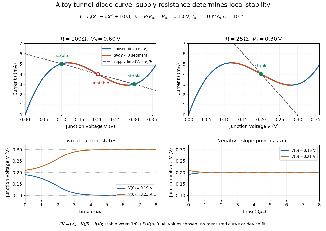
For the second panel, choose and . Now andThere is exactly one real operating point, again . Here , despite the device's own slope . With , the perturbation decays with time constant ; the unstable middle point of the first panel has growth time .
The one-state autonomous model supports switching between attracting operating points after a perturbation or parameter change; it cannot produce a nonconstant periodic orbit. A proposed oscillator needs additional dynamics. This limitation is useful: a load-line intersection establishes a possible steady reading, the slope test establishes local attraction in a specified model, and neither calculation alone predicts an oscillation frequency for a real tunnel diode.
An illustrative abrupt-junction depletion approximation assumes uniform, fully ionized donor impurities and acceptor impurities, negligible mobile space charge in the depleted layer, and permittivity . For area , doping number densities and built-in electric potential difference , it givesHere is the elementary charge and is positive for forward bias. Increasing both doping densities reduces in this estimate. That explains the preparation strategy for a tunnel diode; it does not make this sharp-depletion approximation a precise microscopic model of a degenerate semiconductor.
For a uniformly doped p-n junction whose depleted thickness lies almost entirely on the donor side, Poisson's equation gives . The minimum field obeys . Integrating the triangular electric field profile gives . The external reverse bias is this total voltage minus the built-in junction potential.
Thermal generation of electron-hole pairs within a reverse-biased depletion region can supply a leakage electric current in addition to neutral-region diffusion. For a simple midgap trap with equal electron and hole lifetime parameters, its scale is , where is depletion width and the lifetime parameter. The electric field separates generated carriers. Unlike ideal diode minority-carrier diffusion current, this contribution scales approximately with rather than and can vary with reverse voltage through . Consequently a measured activation energy need not equal the full band gap.
The depletion approximation replaces the junction's transition region by a region without mobile carriers, leaving only fixed ionized dopants. For a uniformly doped abrupt p-n junction, on the p side, on the n side and outside. Charge neutrality gives . Integrating Poisson equation gives the electric field and the electrostatic band bending.
For a planar abrupt p-n junction with ionized densities , p-side width and n-side width , zero external field requires . Integrating Poisson equation gives , with positive denoting forward bias. Therefore has the displayed value, and . The positive depletion capacitance per area is . It equals when and are signed space charges per area. Differentiating a positive charge magnitude with respect to forward voltage instead gives a negative derivative. The square-root law assumes partially depleted regions, negligible mobile charge and no substantial injected-carrier storage.
For a zero-bias abrupt p-n junction, choose the p side at and the n side at . Ionized acceptors and donors remain fixed while mobile electrons and electron holes diffuse and establish a built-in electric field. In the depletion approximation, mobile carriers are neglected on and the net charge density isCharge neutrality gives . The quasi-neutral bulk can have a large mobile carrier density while its net charge density is nearly zero, because fixed dopant charge compensates it. With complete ionization and nondegenerate carriers, equilibrium also gives ; real carrier profiles vary smoothly rather than forming exact step functions at depletion edges.
The incremental capacitance associated with changes of electric charge around a p-n junction. Its depletion contribution is often estimated by , so an independent junction capacitance measurement can constrain the width of the depletion region under the model assumptions. Other stored electric charge, including injected minority carriers, can also contribute to a measured terminal capacitance.
Let each side of a symmetric abrupt p-n junction have thickness , area and doping density . Partial depletion gives . Both sides become fully depleted at . Beyond that point, the ionized dopant charges are fixed, but an incremental terminal voltage changes the electric field uniformly across the full thickness . Gauss's law then gives , up to terminal orientation. The measured positive capacitance approaches rather than vanishing. This geometrical result assumes ideal contacts, negligible mobile carriers, no breakdown and no other series capacitances.
The controlled introduction of impurities to change a semiconductor's charge carrier populations. Donor impurities and acceptor impurities can produce an n-type semiconductor or a p-type semiconductor, respectively; compensation and temperature also matter.
The number of dopant sites per volume. For a roughly homogeneous three-dimensional distribution, the characteristic site separation is of order . This counts introduced sites rather than automatically counting free conduction band electrons: semiconductor carrier freeze-out or compensation can make the mobile carrier density much smaller.
An energy band formed when localized impurity levels hybridize. For hydrogenic donor states, a typical donor separation gives an exponentially small hopping integral and hence an exponentially narrow bandwidth when . An idealized half-filled band with two spin states per donor has spin-summed density of states of order per volume; its Pauli paramagnetism is . That expression requires and does not by itself describe localization or strong Coulomb interactions.
Before using a Maxwell–Boltzmann chemical-potential formula in a doped semiconductor, compare the carrier density to its conduction-band effective density of states. When n is much larger than , a nondegenerate logarithmic estimate is inconsistent. Use Fermi–Dirac statistics or a controlled degenerate expansion instead. A small effective mass strongly reduces and raises the Fermi energy at fixed density, so even an otherwise familiar donor concentration can put the chemical potential inside the conduction band.
At sufficiently low temperature, thermal ionization of shallow dopants becomes inefficient, reducing the mobile carrier density. An acceptor-doped sample may then have many neutral acceptors and few mobile electron holes. Extracting an activation energy requires a model of dopant ionization and compensation; the mobile density need not have the same simple activation exponent in every compensation regime.
Introduction of dopants by accelerating ions into a solid. Their depth distribution, lattice damage and electrical activation depend on implantation and subsequent annealing.
Placing dopants away from the carrier channel to reduce ionized-impurity scattering while supplying carriers.
A two-dimensional electron gas supplied by remote donors in aluminium gallium arsenide and confined on the gallium arsenide side of a heterojunction. An undoped spacer separates ionized donors from mobile carriers, reducing impurity scattering. A conduction-band band offset and self-consistent band bending create the confinement well.
A compensated semiconductor contains both donor impurities and acceptor impurities. In a nondegenerate equilibrium model with both species fully ionized, charge neutrality gives , while the semiconductor semiconductor mass-action law gives . Solving yieldsFor and , and . Numerically the minority concentration is better obtained as than by subtracting nearly equal numbers. If dopants are only partly ionized, replace in charge neutrality by their ionized concentrations and determine the chemical potential self-consistently.
An amphoteric dopant can act as a donor impurity or an acceptor impurity according to its incorporated lattice site or defect configuration. Silicon in gallium arsenide is the standard example: substitution on the gallium sublattice gives a shallow donor, while substitution on the arsenic sublattice gives a shallow acceptor. Its electrical effect therefore depends on growth conditions as well as total silicon concentration.[ref]
Thermal equilibrium concentrations of the amphoteric dopant Si and the associated carrier concentrations in GaAs by Chang-Ho Chen and others. Abstract: neutral and ionized donor species occupy Ga sites; neutral and ionized acceptor species occupy As sites
For a nondegenerate semiconductor with donor density , no acceptors, and donor energy , an occupied donor has two electron spin states while an empty donor has one. Its ionized fraction is therefore . The conduction-band relation gives . Combining charge neutrality, , with the semiconductor mass-action law, , proves the displayed equation.
Its left side increases strictly for and its right side decreases, so there is one physical solution, with . In the freeze-out regime, holes are negligible and solving the quadratic gives . Strong dopant freeze-out reduces this to . An extrinsic plateau requires and , not simply .
The comparison alone does not establish full ionization for arbitrary donor concentration. Localized-level occupation depends on the chemical potential through charge neutrality. If donor orbit radii greatly exceed their separation, an independent isolated-hydrogenic-level model itself fails and overlapping impurity states or band reconstruction are needed. A stipulated extended-carrier density can still define a conductivity calculation, but it must not simultaneously be interpreted as an independently verified dilute-donor equilibrium result.
Substitutional semiconductor doping replaces selected host atoms with impurity atoms on ordinary lattice sites. A shallow donor impurity can supply a mobile conduction electron and remain positively charged; a shallow acceptor impurity can capture an electron and leave a mobile valence hole, remaining negatively charged. In nondegenerate, substantially ionized material, donor-dominated doping raises the chemical potential toward the conduction edge and acceptor-dominated doping lowers it toward the valence edge. Dopants do not create net bulk charge in a neutral sample: fixed impurity charge compensates the mobile carrier charge. Freeze-out, compensation and degeneracy qualify the simplest relation between dopant and carrier densities.
An intrinsic semiconductor has electron and hole densities , so . In a fully ionised, uncompensated n-type sample with , , , andThus a carrier-density ratio alone is not generally the electrical conductivity ratio. If electron mobility is unchanged and electron transport dominates the intrinsic conductivity, it reduces to ; equal electron and hole mobilities instead give . Ionised-impurity scattering can change the doped mobility.
At sufficiently low temperature, donor or acceptor ionization becomes energetically unfavourable. Carriers remain bound to dopants rather than contributing to conduction, reducing the mobile carrier density. This dopant freeze-out is distinct from the high-temperature intrinsic regime, where thermal excitation across the band gap overwhelms the net dopant contribution.
An impurity level is an electronic energy level associated with a dopant or defect in a semiconductor. A shallow donor impurity introduces a level just below the conduction band, and a shallow acceptor impurity introduces one just above the valence band. Under electrostatic band bending, these levels shift with the local band edges in the same material; their occupation is determined relative to the equilibrium chemical potential.
A sequence of bound-to-bound optical transitions of a hydrogenic donor state or hydrogenic acceptor state, converging on a photoionization threshold . For an initially occupied state, ordinary electric dipole transitions reach states; above the threshold, the final carrier can enter a band continuum.
Articles were limited to the first 100 out of 151 total.