Two examples are poly(3-hexylthiophene), P3HT, a conjugated polymer commonly used as an electron donor, and PCBM, a soluble fullerene derivative commonly used as an electron acceptor. Both are organic semiconductors; “organic” does not imply that their transport properties are identical. Their blend is a familiar donor-acceptor photovoltaic model system.
An exciton is a Coulomb-correlated electron-hole pair, electrically neutral overall. Three useful properties are:
- Exciton binding energy: the energy required to separate the correlated pair into unbound carriers. A larger value makes thermal dissociation less effective; dielectric screening and electronic delocalization influence it.
- Spatial extent: the characteristic electron-hole separation or exciton radius. A localized Frenkel-like exciton is small compared with a Wannier-Mott exciton spread over many unit cells.
- Lifetime: the characteristic time before radiative or nonradiative decay. Together with its diffusion coefficient it determines a transport scale, often expressed as in a specified diffusion-length convention.
In many molecular organic semiconductors, limited screening and localization make exciton binding important, so absorption need not immediately produce collectable free charges.
A suitable donor-acceptor heterojunction provides an energetically favourable route from a bound excitation to an interfacial charge-transfer state and then separated carriers. The electron is preferentially transported in the acceptor and the hole in the donor. The interface facilitates dissociation that is inefficient in a single strongly excitonic material; it must also avoid excessive energy loss and rapid interfacial recombination.
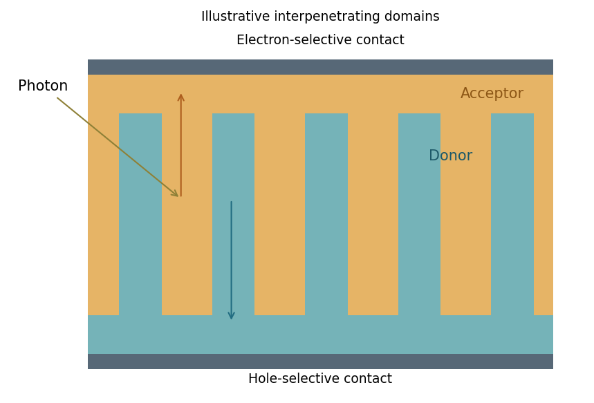
An interpenetrating donor-acceptor structure balances short exciton travel with continuous charge-extraction paths
. Source. Details. 
An idealized bulk heterojunction places most generated excitons within roughly a diffusion length of an interface while maintaining continuous donor paths to the hole contact and acceptor paths to the electron contact. Domain dimensions should therefore be comparable to the material's exciton transport scale, not arbitrarily large. The total absorbing thickness should capture substantial light yet remain within the charge-collection capability set by mobility, field and recombination. Excessive mixing can impair transport or increase recombination; very coarse domains waste excitons before they reach an interface.[ref]
Relative to conventional crystalline-silicon technology, many organic absorbers offer low-temperature thin-film processing and lightweight flexible devices, but have more strongly bound excitons and more disorder-limited charge transport. These are common material trends, not universal statements about every organic or inorganic device.
Relevant semiconductor properties include the absorption spectrum and optical gap, donor/acceptor energy levels and offsets, dielectric screening and exciton dissociation, electron/hole mobilities, recombination lifetimes, traps and morphological stability. Contacts must extract the appropriate carrier selectively. These properties determine the device quantities inA favourable gap alone does not fix efficiency: current generation, voltage loss and fill factor must all be controlled.
Articles by others on the same topic
There are currently no matching articles.