Molecular beam epitaxy is a suitable research-scale choice. Independently controlled elemental beams and shutters allow abrupt composition changes, controlled silicon donor incorporation and thin spacer layers. Growth can proceed sequentially from the GaAs substrate through the undoped GaAs, undoped AlGaAs spacer, doped AlGaAs supply layer and highly doped GaAs cap.
A clean crystalline surface and controlled substrate temperature support epitaxial interfaces; separating the donor layer from the channel is modulation doping. Metalorganic vapor-phase epitaxy can also grow such structures, but MBE's controllable research-scale layer sequence is a strong match to the stated task. Merely depositing the right total elemental amounts would not guarantee the required crystallinity and interface abruptness.
A suitable sequence isFirst pattern the source/drain resist, then deposit and lift off the corresponding metal. Anneal these contacts to produce the low-resistance source/drain interfaces. Remove the exposed cap layer before gate lithography, leaving the cap beneath the contact metal; this uses the contact pads as an etch mask, with suitable protection where required. Finally define and deposit the gate onto exposed AlGaAs and lift off.
The key dependencies are that source/drain metal lands on the n+ cap, the gate lands on AlGaAs after cap removal, and the contact anneal precedes formation of the sensitive Schottky gate. A gate-recess variant can put gate lithography before the local cap etch if that resist is deliberately used as its mask, but it must additionally specify how unwanted conducting cap elsewhere is removed or isolated. The sequence above directly matches the cap remaining only beneath the source/drain contacts in the diagram.
Choose process B, the citric-acid/peroxide wet etch. Its GaAs-to-AlGaAs etch selectivity is , giving strong protection of the underlying barrier and a controllable removal rate for the thin cap.
For comparison, A has selectivity one and therefore no useful etch stop. It is also extremely fast: a nominal GaAs layer would be removed in only . C has selectivity , useful but inferior to B, and clears the same cap in about . D has selectivity four, clears the cap in about and additionally risks plasma-induced surface damage or altered interface properties.
B clears the nominal cap in about . Its slower underlying etch permits a more forgiving endpoint or modest overetch, although actual rates must be checked for the relevant composition and conditions. Wet-etch lateral undercut and contact-metal compatibility still matter; selectivity alone does not make every mask geometry acceptable.
Higher donor concentration moves the semiconductor Fermi level toward the conduction band, reducing the semiconductor work function when these quantities are expressed as energies. Equilibration with the metal aligns electrochemical potentials and creates band bending.
For an ideal n-type Schottky interface the barrier energy is not automatically reduced merely by raising doping. The decisive change is the narrower depletion region:Large allows electrons to tunnel through the thin barrier, reducing the contact resistance and promoting an approximately Ohmic contact. Contact annealing can further modify the local interface and doping. This allows low-resistance source/drain injection while preserving a more rectifying gate contact; real interface-state pinning can modify the ideal work-function picture.
Use equal-width rectangular contact windows in a row with several different edge-to-edge spacings. For positive-resist lift-off, the future metal pads correspond to clear windows in an otherwise chrome-covered mask: exposure removes resist there, and the unexposed background retains resist beneath unwanted metal.
For ordinary ohmic transmission line contact measurement, a conducting strip or isolated mesa of width connects adjacent pads. Measure several spacings so thatThe intercept separates two contact contributions from the sheet-resistance slope. Large enough pad length relative to the transfer length is needed for the simplest contact-resistivity extraction.
Prepare separate arrays on the appropriate surfaces: annealed source/drain metal on the n+ cap, and gate metal on cap-removed AlGaAs. A Schottky gate is nonlinear, so its interface cannot be assigned an ohmic zero-bias contact resistivity merely by fitting the same straight line. Use bias-dependent current–voltage or differential-contact analysis, accounting for the two rectifying contacts.
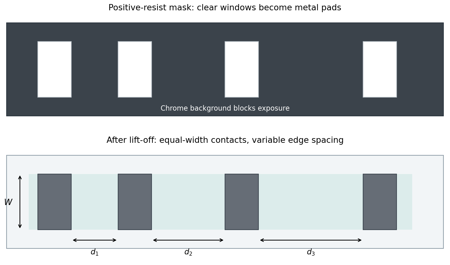
Positive-resist lift-off mask and variable-spacing contact array
. Original schematic. Pale windows in the dark chrome background define future metal pads. The resulting equal-width pads have different edge spacings. Ohmic TLM analysis and bias-dependent analysis of a Schottky contact require distinct electrical models. Details.
Starting from the clean wafer, dehydrate it and use an appropriate adhesion treatment if required. Spin coat the positive resist to obtain a uniform film, then soft bake to remove solvent and stabilize handling. Align the mask and expose the clear pad windows. Develop away the exposed resist, rinse and dry, leaving openings at future metal locations.
Inspect the openings and clear residual resist gently if needed. Perform a compatible surface preparation immediately before metallization so that an unintended oxide or contaminant film does not dominate the contact. Deposit metal with a resist profile and film thickness that leave an accessible discontinuity at the resist edge; an undercut or suitable lift-off stack helps prevent continuous sidewall coating.
Dissolve the sacrificial resist and lift off metal above it, leaving the pads on the exposed semiconductor. Rinse, dry and inspect for residues or bridges. For source/drain test contacts, apply the intended contact anneal; for gate test contacts, preserve the intended Schottky interface. An aggressive final resist hard bake or a fully conformal bridging metal film can defeat lift-off, so these are not automatic extra steps.
Articles by others on the same topic
There are currently no matching articles.