Use clocked processor registers, each storing an -bit word, two independent combinational read ports and one synchronous write port. Each address requires bits. The read addresses select two -to-one multiplexers, each bits wide. A write-address binary decoder combines its selected line with the global write enable to form the individual enables:At the active clock edge, register captures the common write data if , otherwise retaining its word. Reads return the currently stored words selected by their respective addresses. For non-power-of-two , unused address codes need a specified harmless implementation. A simultaneous read and write of one address follows the chosen edge/read timing; an additional forwarding circuit would be needed if a different bypass convention were required.
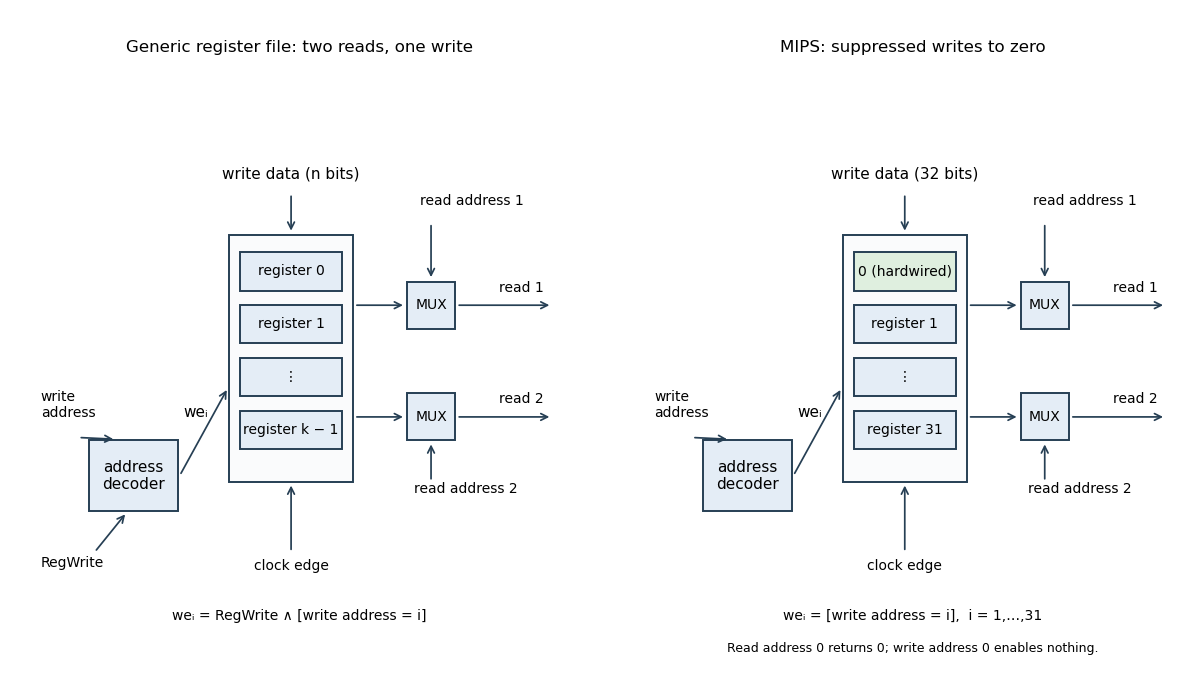
Two-read-port register file with a single synchronous write port
. The left panel uses a global write enable; the right shows the MIPS alternative with writes to index zero suppressed. Both read multiplexers select independently, and the alternative returns a hardwired zero for address zero. Details.
Articles by others on the same topic
There are currently no matching articles.