Use clocked processor registers, each storing an -bit word, two independent combinational read ports and one synchronous write port. Each address requires bits. The read addresses select two -to-one multiplexers, each bits wide. A write-address binary decoder combines its selected line with the global write enable to form the individual enables:At the active clock edge, register captures the common write data if , otherwise retaining its word. Reads return the currently stored words selected by their respective addresses. For non-power-of-two , unused address codes need a specified harmless implementation. A simultaneous read and write of one address follows the chosen edge/read timing; an additional forwarding circuit would be needed if a different bypass convention were required.
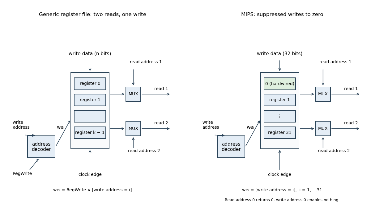
Two-read-port register file with a single synchronous write port
. The left panel uses a global write enable; the right shows the MIPS alternative with writes to index zero suppressed. Both read multiplexers select independently, and the alternative returns a hardwired zero for address zero. Details.
Keep storage only for registers 1 through 31, return a hardwired all-zero word on either read port when its address is zero, and setThere is no enable for register zero and no global RegWrite input to this register file. The right-hand diagram above shows this change. Every clock edge may select a write address; choosing zero suppresses all physical register enables. Consequently the MIPS zero register acts as a write-suppression destination.
Move the no-write decision into the destination-address path. If the original destination selection produced and the original write-enable decision was , drive the new register file withA five-bit two-input multiplexer after the existing destination selector implements this, or the decoder can directly select among zero, the instruction's destination fields and register 31. Its control still distinguishes writing and non-writing instructions: removing the register-file enable pin does not remove that logical decision.
Read-address selection and the result-data path can remain unchanged. Instructions that formerly disabled RegWrite now select destination zero; their write data is irrelevant. Instructions writing an actual destination preserve the same address and data. Since writes to the MIPS zero register were already discarded, the architectural behaviour is unchanged for that case as well.
For
add, select rd and the arithmetic logic unit result. For sw, select destination zero while retaining the memory-store controls and source-register reads. For jal, select register 31 and the return-address data. These are the same actual register writes as before, with sw using destination zero in place of disabling RegWrite. Articles by others on the same topic
There are currently no matching articles.