The internal Boolean functions are , , , and . Put the falling edge of at . Since throughout, throughout. The remaining transitions, including every stated propagation delay, areThe inverter delays the rise of by ten nanoseconds, and the AND gate adds another ten. Consequently and are simultaneously zero for ten nanoseconds. This gap propagates through the two OR gates. The output has a static-one logic hazard: a low glitch on ns, despite its equal initial and final logical values.
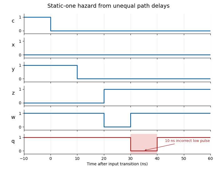
Delayed transitions produce a ten-nanosecond static-one logic hazard
. The shaded interval marks the incorrect output pulse. Exact ten-nanosecond gate delays are used, including propagation of the pulse. Details.
Articles by others on the same topic
There are currently no matching articles.