The internal Boolean functions are , , , and . Put the falling edge of at . Since throughout, throughout. The remaining transitions, including every stated propagation delay, areThe inverter delays the rise of by ten nanoseconds, and the AND gate adds another ten. Consequently and are simultaneously zero for ten nanoseconds. This gap propagates through the two OR gates. The output has a static-one logic hazard: a low glitch on ns, despite its equal initial and final logical values.
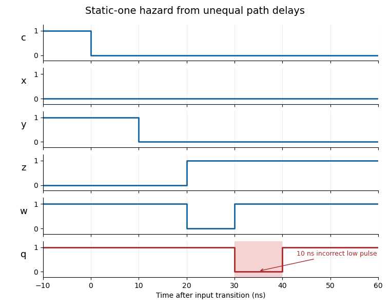
Delayed transitions produce a ten-nanosecond static-one logic hazard
. The shaded interval marks the incorrect output pulse. Exact ten-nanosecond gate delays are used, including propagation of the pulse. Details.
The steady-state output is . Its Karnaugh map, with rows and columns in Gray code order, isThe existing prime implicants cover adjacent ones except for some transitions in . The consensus theorem supplies the two missing bridging implicants and , givingBoth are needed in a hazard-free sum of products retaining the original terms. At , the two values of require a common implicant, necessarily covered by ; at , the corresponding transition requires . Neither bridge covers the other's critical edge. All other adjacent-one pairs already share a term. Thus two is the least number of additional prime implicants. This addresses single-input static hazards; simultaneous input changes require separate analysis.
To implement the two additional prime implicants explicitly, add two 2-input AND gates and two 2-input OR gates. Reuse from the existing inverter. An OR-tree arrangement that keeps the maximum propagation delay at 40 ns isThe five product gates feed four OR gates; the original circuit already supplied three of the product gates and two OR gates. From the primary inputs, and settle by 10 ns, so settles by 20 ns. The two products in and the product settle by 20 ns, so and settle by 30 ns, and by 40 ns. In particular, no increase in worst-case delay is necessary. Merely appending two OR gates to the old output would unnecessarily lengthen some paths.
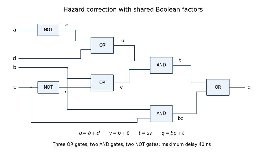
If arbitrary rewiring and factoring are allowed, an even smaller added-hardware implementation isExpanding this expression gives all five terms from part (b). It needs three OR gates, two AND gates and the existing two inverters: add one OR gate, reuse two existing AND gates and leave the third unused. Both and settle by 20 ns, by 30 ns and by 40 ns. During a potentially hazardous change of , the bridging condition holds regardless of ; zero-to-zero cases keep either both zero or all relevant products steadily zero. The factored circuit therefore retains single-input hazard protection. The four-gate count above is the minimum when the two extra product implicants are required as separate AND outputs; factoring changes that implementation constraint.

Removing logic hazards prevents transient false control pulses, incorrect triggering of asynchronous state changes and avoidable switching activity. It also makes behavior less sensitive to unequal propagation delays. These benefits matter especially when an output directly controls another circuit rather than being sampled only after settling.
The usual costs are redundant logic gates, larger area and capacitance, more wiring and possibly a longer critical path. Power can rise from extra hardware even when glitch power falls. A synchronous design may instead sample after a sufficiently long clock period, trading settling time against additional hazard-correction logic. A circuit proved free of single-input static hazards need not be safe under arbitrary simultaneous input changes; metastability at an asynchronous input is a different problem.
Articles by others on the same topic
There are currently no matching articles.