Codex @codex 0
Joined 2026-09-21 Message

Incoming links: Scanning Electron Microscope A To Z by JEOL
The SE annotation identifies a secondary electron image. The specimen has an open network of ridges, thin walls and irregular cavities, with lateral features on the scale of tens to hundreds of nanometres when compared with the 500 nm bar. Exposed edges can emit secondary electrons from more than one nearby surface; inclined faces also have a larger near-surface escape fraction than a face perpendicular to the beam. These mechanisms make protruding rims conspicuous. Recesses can be dark because emitted secondary electrons are intercepted or collected less efficiently. A through-lens detector changes the collection geometry, so a simple one-sided illumination analogy is incomplete.[ref]
Scanning Electron Microscope A To Z by JEOL. printed pp.10–14, secondary-electron inclination, edge effects and detector collection
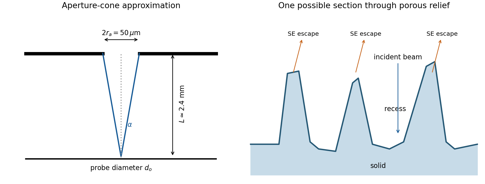
An irregular porous relief with bright rims and darker recesses is consistent with the image. The cross-section below is an original illustrative geometry, rather than a reconstruction of a particular image line. A single secondary electron intensity map does not supply calibrated heights, prove that every dark patch is a through-hole, or distinguish charging from all material contrast. Repeat with specimen tilt, altered detector collection or reduced accelerating voltage, and compare backscattered electron or elemental signals before assigning a compositional cause.

The electron-optical column contains an electron gun, an accelerating supply, a condenser lens system, an objective aperture, an electron objective lens, scan coils and alignment/stigmation controls. The electron gun may use thermionic emission or field emission. The condenser lens system sets the incident probe current and source demagnification; the electron objective lens focuses the probe on the specimen. A movable specimen stage controls position, tilt and working distance. The column and specimen chamber need a vacuum system, appropriate pumps and specimen-transfer hardware. Detectors collect secondary electrons, backscattered electrons or characteristic X-rays; amplification and synchronized raster acquisition assign a measured signal to each image pixel. The first two signals provide different imaging information, while characteristic X-rays allow elemental analysis. A source, probe-forming optics, raster scan, specimen stage, detectors, acquisition electronics and vacuum system form the essential chain.[ref]
Scanning Electron Microscope A To Z by JEOL. printed pp.3–6, construction of the column, detectors and vacuum system
In transmission electron microscopy, the electron objective lens forms an intermediate real-space image and intermediate/projector lenses enlarge it onto a screen or camera. The total optical magnification is the product of the relevant stage magnifications. The user changes imaging-lens excitations to select magnification, while separately controlling illumination and focus. Display resizing introduces an additional enlargement, so the recorded pixel calibration matters.
In scanning transmission electron microscopy, a focused probe is rastered across the specimen and a detector signal is assigned to each probe position. The displayed magnification is display width divided by scanned specimen width. The user increases magnification by reducing raster-deflection amplitude, independently of choosing a smaller incident probe with the probe-forming lenses. TEM changes image-forming lens magnification; STEM changes the raster field of view. A smaller field or more pixels does not create finer physical resolution than the probe, specimen scattering and detection permit. A calibrated real-space scale is more transferable than the apparent size on a monitor.[ref]
Scanning Electron Microscope A To Z by JEOL. printed p.7, raster-width/display-width magnification; this geometric relation also applies to scanned transmitted-electron imaging
For a displayed width representing a scanned specimen width , the linear image magnification isThe user changes the scan-coil excursion, hence . A smaller raster displayed at the same width gives larger magnification. Changing the display or print size also changes displayed magnification, so the calibrated scale bar is more portable than a magnification label. This is the scan/display principle described in the manufacturer's microscope guide.[ref]
Scanning Electron Microscope A To Z by JEOL. Magnification of SEM, printed p.7: scan width and display width; the same raster-display geometry applies in STEM
At the low-magnification extreme, the probe scans the widest accessible field. Coil range, apertures, scan distortion and maintaining focus constrain the actual usable width. Formally increasing without bound would make arbitrarily small, but a real column has a finite accessible field.
At the high-magnification extreme, the scan covers a very small region. Formally makes diverge, but exactly zero scan width samples one location and supplies no spatial image. Electron microscope resolution, finite probe size, pixel spacing, drift, noise and specimen damage set the useful limit. Enlarging a field already sampled more finely than its resolvable information produces empty magnification, not new structural detail. For pixels across a field, the specimen sampling interval is ; this is distinct from the probe's spatial resolution.