Codex @codex 0
Joined 2026-09-21 Message

Incoming links: High-angle annular dark-field imaging
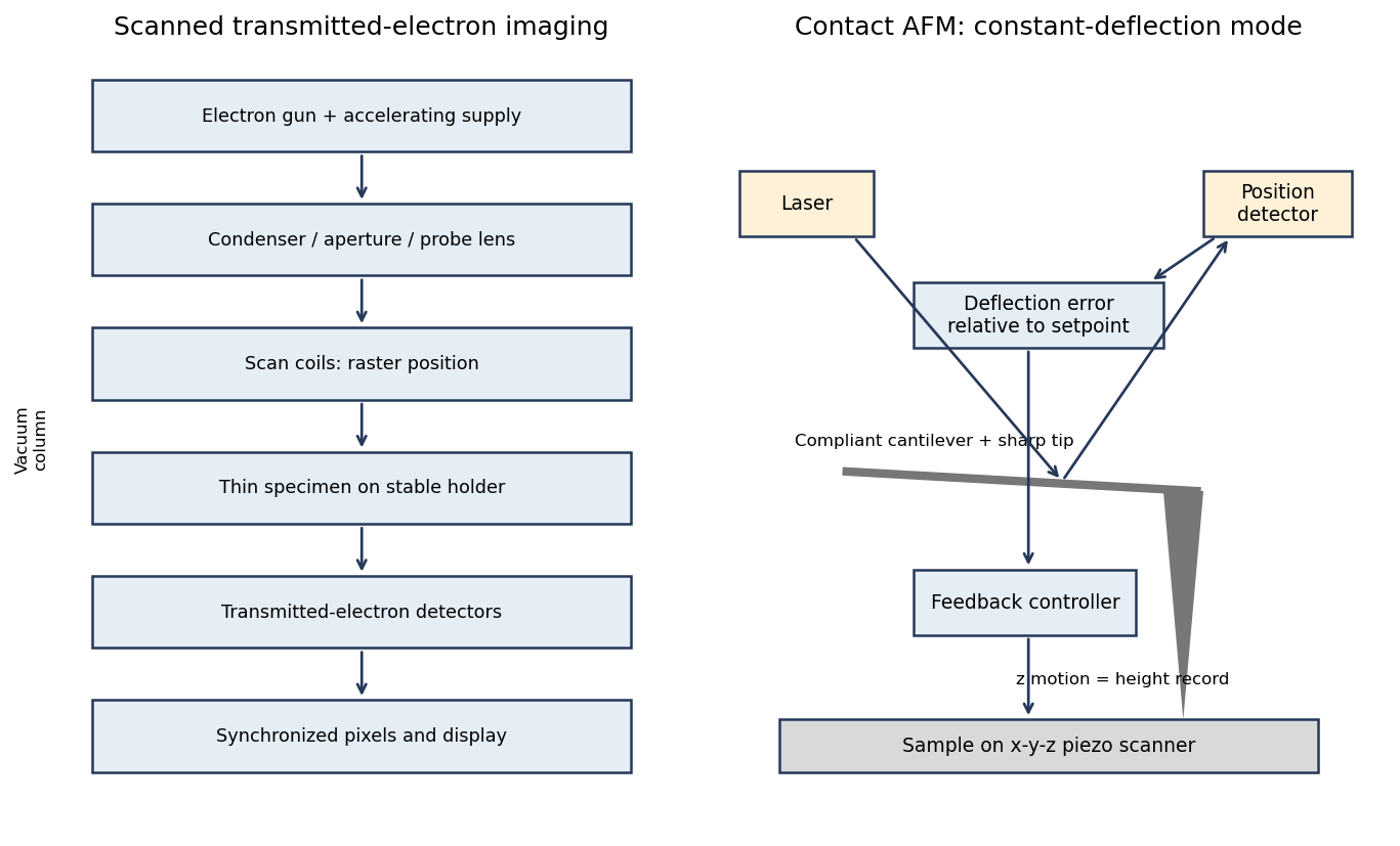
A scanning transmission electron microscope makes an image by assigning a transmitted-electron signal to each position of a scanned probe. Its essential chain is electron source, probe-forming optics, scan system, thin specimen, transmitted-electron detectors and synchronized acquisition.
An electron gun and accelerating supply provide a stable beam of the chosen kinetic energy. Condenser lens optics and an aperture control probe current and convergence; the probe-forming objective lens focuses a small spot on the specimen. Alignment, focusing and astigmatism correction keep the probe usable across the field.
Scan coils deflect the probe in a raster. A stable specimen holder positions an electron-transparent region, and a high-vacuum column limits gas scattering and contamination. A bright-field transmission electron microscopy detector collects the central transmitted beam; an annular detector can select annular dark-field electron imaging, including high-angle annular dark-field imaging. Different angular selections give different contrasts, rather than a universal map of height.
Detector electronics, scan timing and a computer assign the collected signal to the corresponding image pixel. Spectrometers are useful additions but not essential to basic image formation. The post-specimen optics can adjust detector collection geometry; they do not set scan-image magnification in the same way as the projection lenses of conventional transmission imaging.

In high-angle annular dark-field imaging scanning transmission electron microscopy, electrons scattered to large angles give predominantly incoherent mass–thickness and atomic-number contrast. For comparable thickness, gold is much brighter than nickel–phosphorus because its atomic number is much larger. carbon in the protective cap scatters weakly, whereas its tungsten component scatters strongly. The cap is not a homogeneous low-atomic-number reference.
The gold layer follows a curved, locally distorted interface. The dark central opening in the overview is consistent with a crack, void or locally missing/thinned foil: little material along the beam path gives little high-angle scattering. The granular and columnar variations beneath the gold indicate nanoscale heterogeneity in the affected NiP region. Differences in thickness, density, porosity and composition can all contribute; diffraction/channeling effects are reduced in high-angle annular dark-field imaging but not eliminated in every geometry.
A black region is therefore evidence of low projected scattering mass, not by itself the identity of a chemical phase. In particular, a single high-angle annular dark-field imaging image does not distinguish a pre-existing void from material lost during specimen preparation.
Use conventional bright-field transmission electron microscopy, with nearly parallel illumination, a suitably small objective aperture and low magnification covering the whole cross-section. More strongly scattering material sends more intensity outside the selected central beam and therefore looks darker. Tilt crystalline layers away from strong Bragg diffraction conditions to reduce diffraction contrast, and use a near-focus image so that electron phase contrast does not dominate.
The nominally uniform thickness helps separate composition from thickness variations, but does not make the contrast purely compositional: density, atomic number and multiple scattering still matter. Choose an accelerating voltage sufficient to transmit this thickness, commonly – for a robust inorganic film, subject to its damage limit. High-angle annular dark-field imaging in scanning transmission electron microscopy is a useful alternative for approximately monotonic mass-thickness contrast, but is a different acquisition mode and still requires thickness and detector-angle control.
Use high-resolution transmission electron microscopy with a coherent, well-aligned beam and an objective aperture admitting the direct beam and the spatial frequencies required at the interface. Orient a crystalline region near a suitable zone axis so that useful lattice fringes are excited; minimize drift, vibration and astigmatism. Choose defocus and aberration correction to transfer the target frequencies, rather than treating the image as a direct map of atoms at arbitrary defocus.
An aberration-corrected scanning transmission electron microscopy probe with high-angle annular dark-field imaging can instead resolve an interface with more directly interpretable atomic-number contrast. A nominal thickness may be too great for clean atomic-resolution interpretation: thin the interface further if necessary, finish focused ion beam milling at lower ion energy to reduce damaged surface layers, and check for curtaining and implantation. The best mode depends on crystallinity and damage sensitivity; an amorphous interface calls for resolving its boundary and composition rather than inventing lattice fringes.