The infinite exterior potential enforces outside . Within the well,The boundary conditions give and , with . Since , normalization givesThese functions vanish outside the well. The ground state has energy and one density maximum at . The first excited state has energy , a central node, and maxima at . The second excited state has energy , nodes at , and maxima at .
There is no normalized state: that choice gives the zero function. The original wells figure shows all three wavefunctions and probability densities. An arbitrary overall wavefunction sign does not affect the probability distribution.
An isolated nanometre-sized island has small total capacitance , so discrete charge carries appreciable charging energy. A simple constant interaction model isAway from charge degeneracy, adding or removing an electron costs more energy than a sufficiently small thermal/bias window supplies. Coulomb blockade suppresses sequential tunnelling between resolved charge states.
A single-electron transistor has source and drain reservoirs connected to an island through two tunnel junctions, plus an insulated capacitive gate. Each junction has resistance and capacitance; the gate shifts electrostatic energies without carrying the transport current. The original device schematic labels all components.
Require , a source–drain window below the relevant transition, and junction resistances well above to suppress strong quantum charge fluctuations. Electromagnetic noise and lifetime broadening must also be small. Gate-induced charge degeneracy permits conduction even at small bias; there is no gate-independent blockade threshold. Resolving orbital levels additionally requires temperature and broadening below their spacing between energy levels.
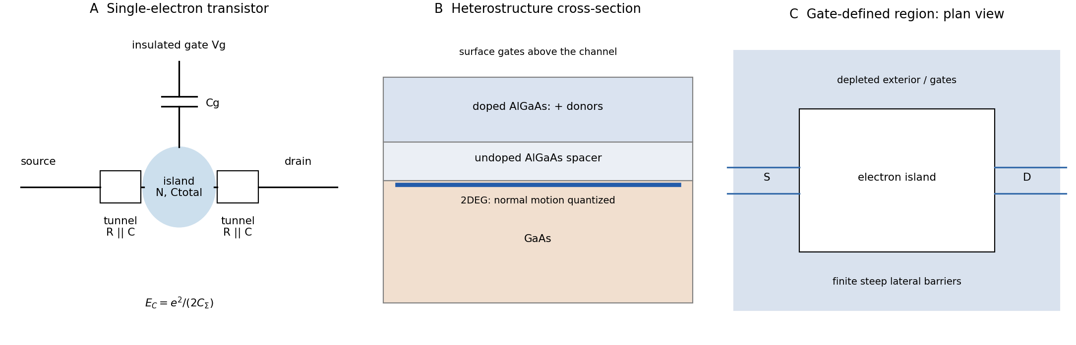

A gallium arsenide/aluminium gallium arsenide semiconductor heterostructure combines lower-gap GaAs with a higher-gap AlGaAs barrier. In a modulation-doped design, AlGaAs donors supply electrons to lower conduction-band states on the GaAs side. An undoped spacer separates the channel from ionized donors and reduces impurity scattering. The interface barrier and band bending quantize motion normal to the interface while allowing in-plane motion: a two-dimensional electron gas.
The normal confining potential is commonly triangular and finite rather than an infinite square well. At suitable density and low temperature, only the lowest normal subband is occupied. modulation doping reduces an important scattering source; it does not eliminate all disorder.
Use negatively biased surface gates to deplete the surrounding electron gas and leave a rectangular central region. Gate voltage controls lateral dimensions and barrier heights. Two constrictions can weakly couple the region to reservoirs, with a plunger gate controlling population. Etched boundaries are possible but may introduce edge disorder. A flat interior and steep edges approximate a box, givingFringing fields, finite barriers and penetration change the ideal result. A 2DEG confines only the normal direction; gates supply the extra lateral confinement. Gate-dependent spectroscopy can test level spacings, while charging measurements separate orbital confinement from Coulomb blockade.
Articles by others on the same topic
There are currently no matching articles.