A semiconductor heterostructure combines different semiconductors, using their interfaces and spatially varying band gaps to control device behavior.[ref]
A difference between the in-plane lattice spacings of joined crystals, which can cause strain and crystal defects during epitaxy.
An intermediate layer used to prepare the growth of a later layer by epitaxy; it need not eliminate the lattice mismatch.
A heterojunction joins different semiconductors; its two sides need not have opposite semiconductor doping.[ref]
A staggered alignment in which the lowest electron states and most favorable hole states occur in different materials. Unlike type-I band alignment, it can reduce electron–hole spatial overlap. Comparing the two band gaps alone does not determine whether this alignment occurs.
A band offset is an interface discontinuity in a conduction band or valence band edge.[ref]
Nobel Lecture: Quasielectric fields and band offsets: teaching electrons new tricks by Herbert Kroemer. §VIII, Fig. 12, pp. 790–791
For a chosen two-material example, let the central material A have and , and the surrounding material B have and , in stipulated energy units. Define positive confinement barriers by and . Then , , and the band gaps obeyThis identity determines the sum of the band offsets; a band gap difference alone cannot determine their partition. The chosen numbers illustrate the definition and do not specify a measured material pair.
A type-I band alignment confines electrons and electron holes together: its inner conduction band edge is lower, its valence band edge higher.[ref]
Nobel Lecture: Quasielectric fields and band offsets: teaching electrons new tricks by Herbert Kroemer. §IV, Figs. 6–8, pp. 786–787
In the chosen band offset example, the electron barrier is , while the electron hole barrier is . A hole's excitation energy is measured downward from a valence band maximum: reversing that convention would incorrectly make the two barriers appear to repel opposite carriers. An electrostatic shift moves both electron energy band edges together; changing the band gap also changes their separation. Thus material composition supplies a control beyond the electric potential alone.
A double heterostructure sandwiches one semiconductor between two layers of another, for example gallium arsenide between aluminium gallium arsenide layers. Suitable band offsets confine injected charge carriers centrally.[ref]
A double heterostructure laser electrically pumps its central layer for stimulated emission. Band offsets confine charge carriers; refractive index contrast confines the optical normal mode.[ref]
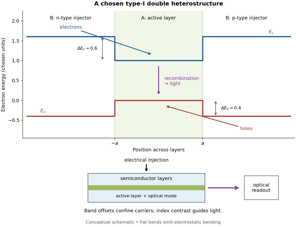
Chosen type-I band alignment: carrier injection and optical readout
. Original schematic using stipulated energy units. The upper panel plots electron energy band edges across the layers; the lower panel separates electrical pumping from the emerging light. Flat segments omit band bending. The curves do not reproduce a historical device. Source. Details.
For an original bookkeeping model, let be the injected pair rate per unit area, the active-layer thickness, its excess pair number density, a recombination lifetime, and an escape time. Before appreciable stimulated emission, supposeChoose two otherwise identical devices with and . The resulting steady state populations are and : improved confinement raises the population by a factor at fixed injection. This linear model assumes equal excess electron and electron hole densities, fixed lifetimes, and no laser gain clamping.
Optical confinement enters separately. For a chosen optical normal mode, define as its gain-overlap factor with the active layer. With material optical gain , internal loss , and mirror loss , a simple laser threshold condition isFor stipulated losses in inverse-length units, requires , whereas requires . This calculation varies optical overlap only; the preceding population calculation varies carrier escape only. Their combination explains the usefulness of controlling both the energy band profile and the optical normal mode.
Herbert Kroemer proposed the double heterostructure laser in 1963; he did not participate in its 1970 experimental realization.[ref]
Nobel Lecture: Quasielectric fields and band offsets: teaching electrons new tricks by Herbert Kroemer. §IV, p. 787
Zhores I. Alferov describes his group's independent 1963 proposal and later experimental program.[ref]The experimental distinction is concrete. A 1962 gallium arsenide p-n junction laser used top and bottom contacts, parallel polished faces, and current pulses with the device in liquid nitrogen. An infrared image converter recorded the radiation pattern; a spectrometer measured narrowing above laser threshold. Comparing the same device below and above laser threshold supplied a control. Pulsed, cooled operation did not demonstrate continuous operation at room temperature.[ref]
Zhores I. Alferov's 1970 team photolithographically patterned stripe double heterostructure lasers on silver-covered copper plates. He reports sustained laser emission at room temperature; Fig. 4 shows the device structure. Independently, Izuo Hayashi, Morton B. Panish and collaborators demonstrated continuous double heterostructure laser operation with diamond heat sinks.[ref]
The below-threshold comparison tests the onset of stimulated emission; continuous operation additionally requires sustained removal of waste heat. Neither observation alone measures the separate band offsets, optical overlap, or every loss mechanism. The schematic above therefore explains a design principle rather than reconstructing the historical apparatus.
A quantum well confines a particle in one spatial direction while allowing motion along the layer. In a semiconductor heterostructure, band offsets can create that confinement. The following finite square well model makes the resulting discrete transverse energy levels explicit.
For one nondegenerate thermalized particle, excited-state occupation relative to the ground state is set by the excitation gap, not by the absolute energy origin. In an infinite square well of width , the first gap is . Predominant ground-state occupation requires this gap to be much larger than ; an explicit tolerated occupation gives a quantitative temperature criterion. State quantum degeneracy adds its statistical weight.
An electric field normal to a semiconductor quantum well shifts the electron and hole confinement energies and displaces their envelopes in opposite directions. The exciton optical transition usually redshifts and its oscillator strength falls as their overlap decreases. In a symmetric unbiased well the permanent dipole vanishes, so the leading weak-field shift is quadratic. This optical shift includes confinement and binding changes; it is not solely a change in exciton binding energy.
For parabolic bands confined by an infinite well of width , a same-index transition has edge . Above it the in-plane pair kinetic energy is with reduced mass .
In an infinite square well, electron and hole envelopes are the same normalized sine functions even when their effective masses differ. In the electric dipole and envelope approximations, their overlap is . The same-index rule is an ideal-envelope rule, separate from Bloch-state polarization selection rules.
A semiconductor state is approximated by a slowly varying envelope multiplying a cell-periodic Bloch function from a selected band. effective masses govern the envelope equation. Interband optical matrix elements then factor approximately into a cell-scale momentum matrix element and an envelope overlap; abrupt interfaces, band mixing and nonparabolicity limit the separation.
Consider an original one-dimensional effective mass model with for and outside. Take the same positive effective mass everywhere, an abrupt interface, and no interactions. The wavefunction represents a transverse envelope; free motion parallel to the layer is outside this calculation. A double heterostructure laser need not be thin enough for this quantization to dominate its operation.
Set , , , and . The time-independent Schrödinger equation becomesHere denotes the dimensionless potential; a bound state has . Matching the wavefunction and its derivative at givesFor the even bound state, the interior solution is and the exterior solution is . For the odd bound state, replace by and by . The physical wavefunction is .
Wavefunction normalization includes both exterior tails, not just the active layer. Direct integration givesThe first two terms are the interior integral; the last is the total exterior integral. Thus the interior probability is , with the upper sign for even parity.
Choose . There is one even root in and one odd root in ; higher branches start beyond . Each left-hand side increases on its stated interval while decreases, proving uniqueness there. Numerically,These are calculated values of the chosen finite square well. The excited bound state lies closer to the barrier and has a longer exterior tail: being bound does not mean having unit probability inside the well.
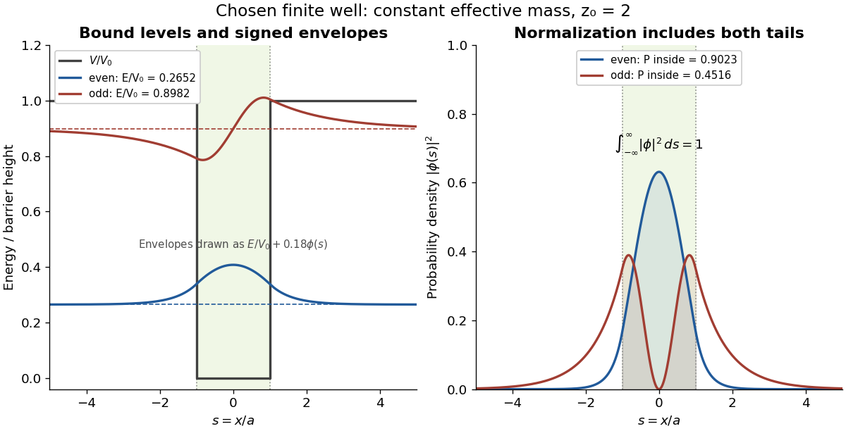

This model demonstrates electronic confinement, not optical refractive index confinement or a complete laser. Unequal effective masses, band bending, interface disorder and interactions require a more detailed model. In particular, continuity of the ordinary derivative above uses the chosen constant effective mass assumption.
Articles by others on the same topic
There are currently no matching articles.