Absorbed photons with energy at least the band gap generate electron–hole pairs. The built-in field of the p-n junction separates carriers generated in or reaching the depletion region; minority carriers generated nearby can diffuse into that collection region. Selective contacts carry electrons and holes into an external circuit before they recombine.
Define positive electric current into the positive-voltage terminal. In the ideal illuminated-diode model,The dark curve has ; illumination shifts it downward. At short circuit ; at open circuit and . Between them the illuminated cell lies in quadrant IV and supplies power . The maximum power point maximizes the area of the rectangle with sides and :It is neither the open-circuit point nor the short-circuit point, both of which supply zero power.
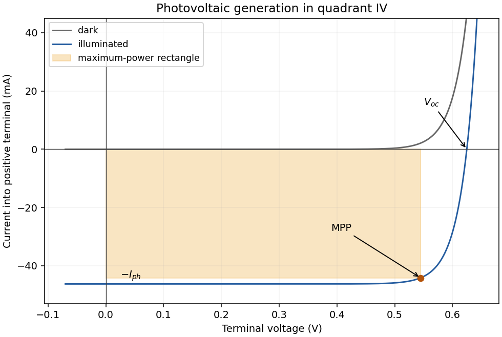

At fixed spectrum and temperature, photocurrent is approximately proportional to irradiance, so the magnitude of short-circuit current increases nearly linearly. In the ideal model,so open-circuit voltage rises only logarithmically with irradiance. More incident optical power generally raises the maximum electrical power, within the device's thermal and resistive limits.
Increasing temperature strongly increases the dark saturation electric current. In silicon this normally reduces open-circuit voltage and maximum power, despite a small increase in short-circuit current associated with the temperature dependence of absorption and band gap. The thermal-voltage factor alone is insufficient to predict the sign; the temperature dependence of matters.
maximum power point tracking adjusts the load seen by the cell as irradiance and temperature change. A controlled DC–DC converter can transform the external load so that operation stays near the changing maximum of , instead of at the generally suboptimal intersection with a fixed load. It matches operating conditions and cannot generate additional energy beyond the photovoltaic output.
Articles by others on the same topic
There are currently no matching articles.