A transparent metallic network must span the patterned electrode with many redundant current paths while obscuring little area. For random rods, number density times squared wire length is a useful percolation measure; greater aspect ratio generally reaches a connected network at lower coverage. Conductivity also depends on intrinsic metal resistivity, wire cross section, orientation, length distribution, wire–wire contact resistance and the number of junctions along each spanning path. Insulating capping layers can make nanowire junction resistance dominate even when the individual wires are excellent conductors.
Near the connectivity threshold, small density changes or wire breaks produce large resistance changes. For a narrow stripe, finite-size effects and orientation matter: a macroscopic sheet-average percolation result does not ensure a reliable 100 µm-wide path. Optical performance depends on coverage, metal extinction, wire diameter, aggregation, optical haze, substrate transmission and any binder. Increasing wire density lowers resistance but usually lowers transmission. Welding, pressing or suitable embedding can improve contacts with less additional optical coverage than simply adding metal.[ref]
Self-limited plasmonic welding of silver nanowire junctions by Erik C. Garnett and others. Nature Materials 11 (2012), pp. 241–249, junction-localized welding mechanism
The stripe has squares, so its end-to-end resistance is ; the stated sheet-resistance limit requires a stripe resistance below 5 kΩ, not 20 Ω. The sketch below separates sparse connectivity, redundant paths and junction quality.
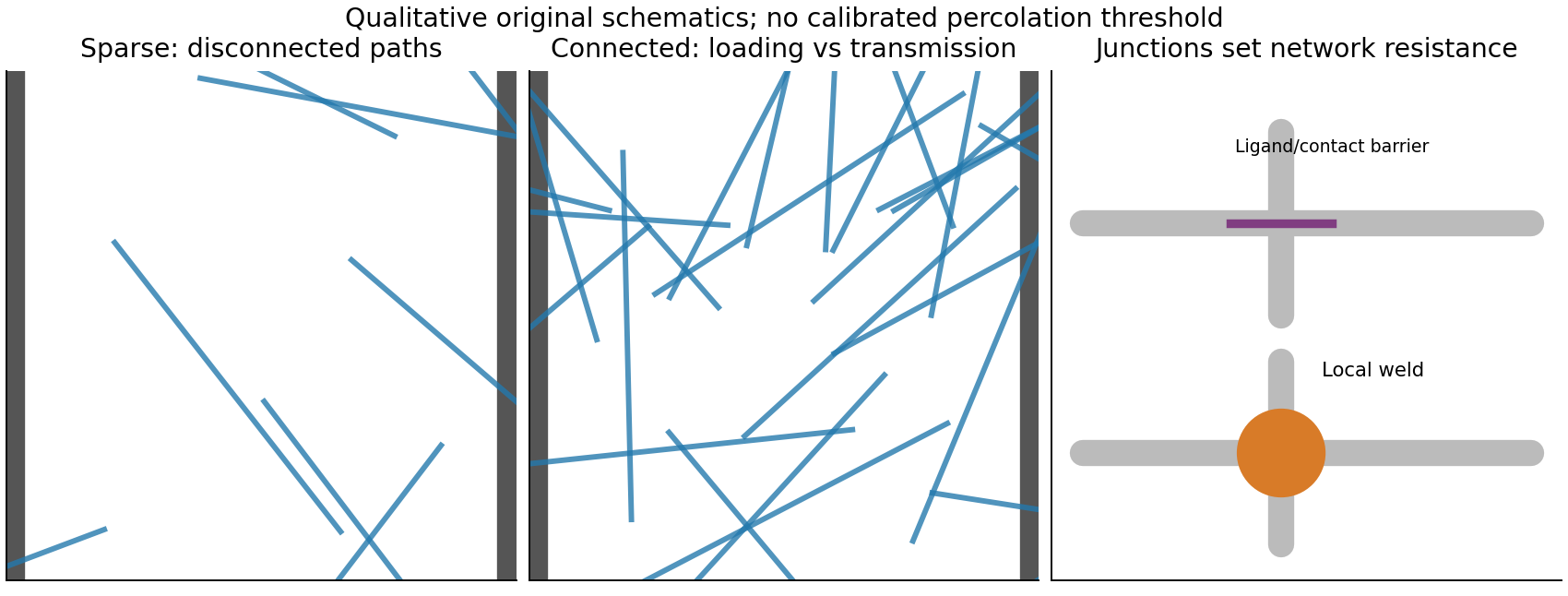
Original network schematics distinguishing connectivity, optical coverage and wire-junction resistance
. Details. 
Three credible architectures are a welded silver nanowire network; a thin silver nanowire network with a conducting polymer overcoat; and a nanocrystalline silver grid formed from nanoparticle ink. Silver provides low intrinsic resistivity. A sparse long-wire network can be both flexible and highly transmitting if its junctions are well connected. A thin, optically weak conducting polymer overcoat can bridge junctions and smooth the surface, provided its added absorption and moisture sensitivity are controlled. A fine grid offers a more directly designed optical/electrical trade-off and does not rely on operating near random percolation.
For a quantitative grid feasibility screen, take pitch , line width and metal thickness . An opaque-line square-grid estimate gives . With a transmitting polymer substrate of 0.95, the combined estimate is 0.912. The sheet resistance is approximately . Even an effective silver resistivity four times gives , with a coating thinner than 400 nm. There are about 20 mesh periods across the stripe, making the finite-width design more credible than a pitch comparable with its whole width.
These are feasible material/process choices, not guaranteed specifications for every film carrying those names. For the two nanowire architectures, choose wire dimensions, loading and junction treatment to pass the same finished-stripe measurements; the hybrid's optical budget must include its overcoat. Measure transmission at 550 nm with its reference stated, sheet resistance, profile thickness, bend-cycle stability and pattern continuity. Bare nanotube or graphene networks should not be assumed to meet this demanding resistance–transmission combination without additional metallic conduction or other demonstrated improvement.
For the silver nanowire network, synthesize or source long, narrow wires, remove excess ligand without causing aggregation, formulate a stable coating ink and coat the flexible web by a scalable method such as slot-die coating or gravure printing. Dry below the substrate's damage temperature, then press or locally weld junctions and embed or cap the network if required. Define 100 µm stripes by masked coating, a printing-compatible patterned wetting layer, or post-coating laser ablation; provide robust end contacts and remove stray bridges between adjacent stripes. Roll processing offers throughput, but coffee-ring effect, wire alignment, random weak links and ablation damage require inline optical/electrical inspection. Verify that the local junction treatment improves resistance without simply darkening the whole film.
For the silver nanoparticle-derived grid, use a repeatable nanoimprint lithography to form a fine mesh inside the outer 25 mm by 100 µm stripe pattern. Fill the channels with a silver nanoparticle ink, remove excess from the transparent openings, and consolidate the metal by substrate-compatible chemical, photonic or low-temperature thermal sintering. Transfer or embed the grid into the polymer surface and add electrical pads. The quantitative design in part (b) sets target pitch, line width and thickness; the large-scale process must maintain those dimensions and a continuous metal cross section. A master enables repeated replication and deterministic open area, but tooling cost, incomplete filling, residual metal in windows, shrinkage cracks, imperfect sintering and adhesion are important limitations. Test the finished patterned stripes, rather than relying on a large unpatterned test coupon alone.
Articles by others on the same topic
There are currently no matching articles.