For a uniformly magnetized bilayer that relaxes to one of its easy directions after a saturating in-plane field, the in-plane remanent component isIt is therefore approximately zero when the easy axis is perpendicular at the thin-Co end, and increases towards as the easy axis rotates into the plane. The graph should show an increasing crossover between about and , but the source does not specify its exact shape. A straight line is not a consequence of the two endpoint orientations.
The trend reflects competition between interface-driven perpendicular magnetic anisotropy and volume or demagnetizing contributions favouring in-plane magnetization. An illustrative effective anisotropy is , with sign convention chosen so positive favours the normal. A continuous rotation can require higher-order anisotropy terms; the simple sign change alone need not produce a smooth canting interval.
The relation assumes a well-defined remanent direction and no complete cancellation by domains. A vibrating-sample magnetometer measures total moment: if the result is reported without dividing by magnetic volume, the moment per area additionally scales as .
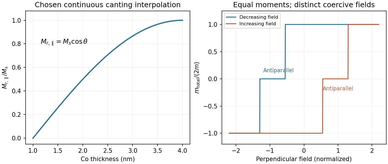
Illustrative remanence crossover and independent two-layer magnetic switching
. The remanence interpolation is a chosen schematic, not fitted data. The hysteresis loop assumes equal magnetic moments, distinct coercivities and independent abrupt reversal. Details.
Let the two layers have equal magnetic moments and coercive-field magnitudes . Assume they are exchange-decoupled, both easy axes are perpendicular, each switches sharply, and dipolar coupling, thermal activation and domain distributions do not smear or offset reversal.
Starting from positive saturation and reducing the perpendicular field, the total moment changes asat and . Between the switches, the moments are antiparallel and cancel. On the return sweep the corresponding transitions occur at and . The plotted normalized loop therefore has two reversal steps and an antiparallel plateau on each sweep, as in the accompanying figure.
Equal magnetization densities do not alone guarantee an exactly zero plateau if the two Co thicknesses or active areas differ: cancellation requires equal moments . The source allows Co thickness variation, so this is an additional assumption worth stating. A real unpatterned millimetre-scale film may reverse by domain processes rather than coherent rotation, producing rounded steps and reduced remanence.
In current-perpendicular-to-plane magnetoresistance, the resistance difference between parallel and antiparallel ferromagnetic layers relies on spin-dependent transmission and retention of spin information. Here, an electron traversing the stack must pass a platinum layer between the two Co films. Strong spin-orbit coupling and associated spin relaxation in Pt, together with spin-memory loss at interfaces, can reduce the polarization reaching the second Co layer and weaken giant magnetoresistance. This is more relevant to the stated perpendicular current than an in-plane shunting explanation.
First, redesign the spacer path so a low-spin-relaxation conductor such as Cu directly separates the two ferromagnets, while retaining perpendicular anisotropy through other interfaces or a different layer sequence. Minimize unnecessary Pt traversal and improve interface sharpness. Merely thinning the Cu layer is not sufficient if it reintroduces magnetic coupling or leaves the Pt spin-relaxation bottleneck unchanged.
Second, replace the metallic spin-transport section with a suitable thin insulating tunnel barrier, for example an engineered MgO-based magnetic tunnel junction, and choose compatible magnetic electrodes. Spin-selective tunnelling can give a much larger resistance contrast, but pinholes, disorder and a poorly matched barrier defeat it. Retaining distinct switching fields and a stable antiparallel configuration remains essential in either design.
A gallium arsenide/aluminium gallium arsenide heterojunction has a conduction-band offset that can confine electrons on the GaAs side. Donors in the wider-gap AlGaAs supply electrons; band bending produces a narrow interfacial potential well. Motion normal to the interface is quantized into subbands, while motion within the plane remains approximately free with GaAs effective mass. Occupying the lowest confinement subband creates a two-dimensional electron gas.
Modulation doping spatially separates the ionized donors from the mobile electrons. An undoped spacer between the donor layer and the channel reduces Coulomb scattering from donor ions while still allowing charge transfer. This can produce higher mobility than doping the conducting channel itself. The spacer thickness balances lower scattering against weaker carrier supply and electrostatic control; interface roughness, alloy disorder, phonons and background impurities can still limit mobility. The channel is a finite-width quantum wavefunction, not a mathematically zero-thickness sheet.
For an in-plane parabolic band , one state occupies area in two-dimensional wave-vector space. Including spin degeneracy two and the single GaAs conduction-band valley,Differentiation gives the constant two-dimensional density of statesUsing the supplied and effective mass givesThis counts available one-electron states, not the number actually occupied at arbitrary temperature. Occupation requires the Fermi-Dirac distribution; each additional subband would add another step above its own threshold.
Interpret the stated Fermi energy as measured above the bottom of the occupied subband, and take a degenerate, nearly zero-temperature gas. ThenFor a filling energy,A Fermi energy referenced instead to an unspecified bulk conduction-band edge would not determine this number without the subband offset. The assumption that only one subband is occupied is imposed by the question; at this comparatively large density, an actual confinement potential should be checked before applying it to a device.
Treat the metal gate and conducting electron sheet as a parallel-plate capacitor separated by a uniform GaAs-like dielectric. Its capacitance per area isA gate-voltage change gives an electron-number change of magnitudeFor the ordinary accumulation convention, a more positive gate voltage attracts more electrons, while a more negative gate depletes them. The magnitude is about of the preceding sheet density.
This neglects depletion, trapped charge, finite well width and quantum capacitance. The occupied-subband quantum capacitance is , much larger than here; putting the two in series would reduce the estimate by only about within this simple model.
Articles by others on the same topic
There are currently no matching articles.