Source: NanoMPhil Paper 2 2022.pdf, physical pages 1–14 of that ZIP member; questions occupy pages 3–14.
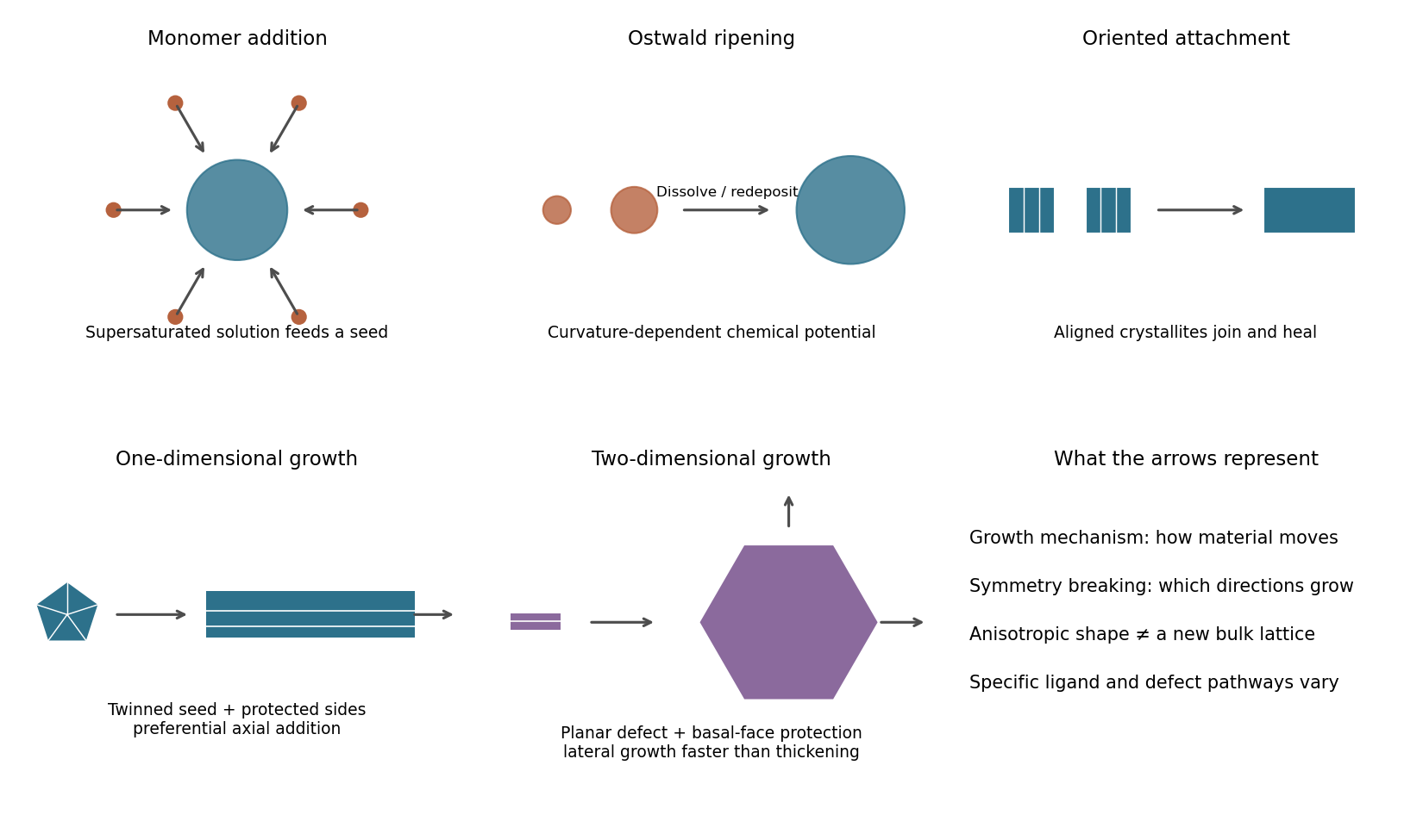
Three useful growth mechanisms are monomer addition, Ostwald ripening and oriented attachment. They can occur sequentially or compete; they are not necessarily three distinct experimental recipes.
In monomer-addition crystal growth, dissolved atoms, ions or molecular growth units attach to an existing nanocrystal. Supersaturation provides a chemical-potential driving force, approximately for an ideal solution. Transport through solution and incorporation at steps or facets determine the rate. Growth consumes the excess solute without requiring collisions between whole crystals.
In Ostwald ripening, smaller crystals dissolve while larger ones grow through solution. Curvature raises the surface contribution to chemical potential, approximately for a sphere with surface free energy and atomic volume . Dissolved material therefore moves from high-curvature particles to lower-curvature ones, reducing total interfacial free energy.
In oriented attachment, whole crystallites align compatible lattice planes and join. Removing exposed surface and forming a coherent interface lowers free energy; rotation, ligand removal and interface healing can be rate limiting. Misalignment can leave twins or other defects. Simple aggregation without crystallographic registration is related particle attachment, but is not necessarily oriented attachment.

Symmetry breaking in nanocrystal growth makes growth rates along initially equivalent crystallographic directions unequal, so the final shape has lower symmetry than an unperturbed seed. It need not change the underlying face-centered cubic lattice. A cubic lattice does not require a cubic external shape.
Anisotropy can originate in a twin or stacking fault, unequal ligand coverage of nominally equivalent sites, selective adsorption or etching, a substrate or external field, or a local fluctuation amplified because newly deposited material changes subsequent growth. Facet-selective binding suppresses some normal growth rates; concentration and reduction kinetics determine whether atoms can redistribute towards a near-equilibrium shape or remain in a kinetically selected one. A facet with slow normal growth tends to remain exposed, while a fast-growing facet can disappear.
For a one-dimensional silver example, begin with a small seed with multiple regions related by crystal twinning containing five sectors around a common axis. Ligand-protected lateral faces and more active ends favour axial addition, producing an elongated pentagonal rod and then a wire. The defect geometry and surface kinetics jointly distinguish the axial direction. Fivefold twinning is a composite structure with strain accommodation, not a perfect single fcc crystal with forbidden fivefold lattice symmetry.
For a two-dimensional example, begin with a seed containing a planar twin or stacking fault. Basal-face protection and enhanced incorporation at suitable edges favour lateral extension over thickening, producing a thin triangular or hexagonal plate. The accompanying schematic emphasizes seed, symmetry-breaking event and anisotropic growth stages. These are representative routes, not universal requirements for every rod or plate. Experimentally, silver-seed growth can also be redirected into lower-symmetry forms by controlling reduction kinetics.[ref]
Symmetry Breaking during Seeded Growth of Nanocrystals by Xiaohu Xia and Younan Xia. 2012, seeded-silver growth and kinetic symmetry breaking
In surface-enhanced Raman spectroscopy, electromagnetic SERS enhancement comes from the strong local optical field near a plasmonic metal nanostructure. A localized surface plasmon resonance in gold or silver can increase both the field driving a molecular Raman transition and the coupling of its emitted light to the far field. A common estimate isoften summarized as an enhancement when pump and Stokes frequencies see similar responses. Sharp tips and narrow interparticle gaps can produce intense hot spots.
Chemical SERS enhancement changes the molecule's Raman polarizability through adsorption, electronic hybridization or a metal–molecule charge-transfer resonance. It is more sensitive to molecular identity and binding geometry than a purely electromagnetic field enhancement, and generally requires close contact.
Tune particle size, shape and gap geometry so that a plasmon resonance overlaps the excitation and Raman frequencies, and bring the target into the enhanced-field region. Reproducible adsorption sites, low fluorescence background and clean reference spectra are as important as a large local enhancement. A hot spot does not guarantee that a dilute sample occupies it; a detection limit cannot be computed from concentration alone. Au or Ag improve the signal per suitably located molecule, while sampling and background determine the practical limit.
In atomic layer deposition, expose the surface to a molybdenum precursor, purge unreacted precursor and volatile products, expose it to a sulfur reactant, and purge again. Each half-reaction should saturate the available reactive sites rather than continue indefinitely with dose. Repetition builds a molybdenum disulfide film, with nucleation, incubation and layer closure checked independently.
Self-limited surface chemistry is not the same as depositing exactly one complete crystal monolayer per cycle. A cycle may add only a fraction of a layer, and initially isolated islands can thicken before all bare substrate is covered. Reactions on hydroxylated silicon dioxide can also differ from those on the comparatively inert MoS basal surface. A precursor pair must actually show saturation under the chosen conditions; simply alternating gases is insufficient evidence of ALD.
In metalorganic chemical vapor deposition, metalorganic and sulfur-containing precursors are typically supplied simultaneously or with overlapping residence times, and film growth depends on decomposition, transport and surface reaction rates. Both methods involve chemistry, but ALD separates saturating half-reactions and purge steps. An ALD process need not use a metalorganic precursor, and pulsed CVD is not automatically ALD.
Potential advantages are reproducible thickness increments, large-area uniformity, conformal access to features and compatibility with moderate-temperature integration. Saturated exposure can make coverage less sensitive to small precursor-flux variations than an unsaturated deposition rate. The cycle count provides a useful process variable for matching an optical or electrical thickness target.
For a monolayer device, control of nucleation and coalescence is especially valuable, because excessive second-layer growth and uncovered patches both change the optical response. The advantages are conditional: a reliable ALD window and suitable precursor chemistry are required, and conformality does not imply a single-crystal film. Long exposure and purge steps reduce throughput, residual ligands or impurities can remain, and post-growth crystallization may require temperatures that the integrated device cannot tolerate.
Many independently oriented nuclei form on an amorphous support and then coalesce before they can become one large crystal. The SiO substrate provides no unique epitaxial orientation. At relatively low deposition temperature, short surface diffusion lengths and slow bond rearrangement restrict the distance over which deposited species can find a well-ordered configuration. Island collisions therefore leave grain boundaries; precursor residues and incomplete sulfurization can add disorder.
Raising temperature or annealing can improve crystallinity, but may conflict with the ALD reaction window, substrate compatibility or sulfur retention. Small grains are consequently a frequent process outcome, not a fundamental theorem that ALD can never form a well-ordered layer. A direct ALD experiment on SiO-covered wafers found nanocrystalline MoS by diffraction and electron microscopy, while demonstrating self-limited precursor exposure behaviour.[ref]
Wafer-scale, conformal and direct growth of MoS2 thin films by atomic layer deposition by Yujin Jang and others. 2016, SiO2 substrates, self-limited growth and nanocrystalline microstructure
The pressure is . The molecular arrival flux from an ideal gas isBecause the residual-gas composition, temperature and sticking probability are not specified, the answer is an order-of-magnitude monolayer-equivalent exposure time, not a unique coverage prediction. Take , a nitrogen-like molecular mass , and unit sticking probability. ThenUse the given molecular-layer scale as an approximate intermolecular spacing, giving . ThusFor , this is a few minutes; assuming instead sites gives about , the same rough scale. A clean-looking vacuum pressure does not imply a contamination-free surface. Desorption and a small sticking probability can greatly lengthen net accumulation, while residual water or hydrocarbons can dominate the chemistry. Full saturation in a site-blocking adsorption model is not exactly the same as one monolayer-equivalent incident fluence.
Use a thin, continuous cap of hexagonal boron nitride, preferably assembled without exposing the cleaned MoS surface to ambient contamination. It is chemically inert and relatively transparent in the visible range, and can isolate the film from adsorbing water, oxygen and hydrocarbons during optical measurements. A transferred sheet avoids depositing a strongly reactive precursor directly on the monolayer.
The cap must cover the illuminated region and overlap its edges; pinholes, wrinkles and unsealed edges can allow ingress. Trapped residues or bubbles can themselves change the optical response. Record the capped background and account for optical interference and dielectric-environment shifts rather than assuming that encapsulation leaves every spectral peak unchanged. A thin oxide or polymer coating may also provide protection, but deposition damage, optical background and permeability require checking. An atomically thin sheet with a perfect basal plane is not proof that the whole assembled enclosure is sealed.
For a uniformly magnetized bilayer that relaxes to one of its easy directions after a saturating in-plane field, the in-plane remanent component isIt is therefore approximately zero when the easy axis is perpendicular at the thin-Co end, and increases towards as the easy axis rotates into the plane. The graph should show an increasing crossover between about and , but the source does not specify its exact shape. A straight line is not a consequence of the two endpoint orientations.
The trend reflects competition between interface-driven perpendicular magnetic anisotropy and volume or demagnetizing contributions favouring in-plane magnetization. An illustrative effective anisotropy is , with sign convention chosen so positive favours the normal. A continuous rotation can require higher-order anisotropy terms; the simple sign change alone need not produce a smooth canting interval.
The relation assumes a well-defined remanent direction and no complete cancellation by domains. A vibrating-sample magnetometer measures total moment: if the result is reported without dividing by magnetic volume, the moment per area additionally scales as .
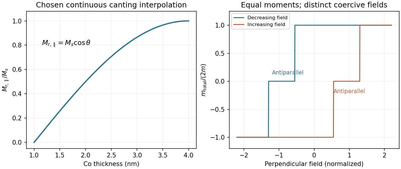
Illustrative remanence crossover and independent two-layer magnetic switching
. The remanence interpolation is a chosen schematic, not fitted data. The hysteresis loop assumes equal magnetic moments, distinct coercivities and independent abrupt reversal. Details.
Let the two layers have equal magnetic moments and coercive-field magnitudes . Assume they are exchange-decoupled, both easy axes are perpendicular, each switches sharply, and dipolar coupling, thermal activation and domain distributions do not smear or offset reversal.
Starting from positive saturation and reducing the perpendicular field, the total moment changes asat and . Between the switches, the moments are antiparallel and cancel. On the return sweep the corresponding transitions occur at and . The plotted normalized loop therefore has two reversal steps and an antiparallel plateau on each sweep, as in the accompanying figure.
Equal magnetization densities do not alone guarantee an exactly zero plateau if the two Co thicknesses or active areas differ: cancellation requires equal moments . The source allows Co thickness variation, so this is an additional assumption worth stating. A real unpatterned millimetre-scale film may reverse by domain processes rather than coherent rotation, producing rounded steps and reduced remanence.
In current-perpendicular-to-plane magnetoresistance, the resistance difference between parallel and antiparallel ferromagnetic layers relies on spin-dependent transmission and retention of spin information. Here, an electron traversing the stack must pass a platinum layer between the two Co films. Strong spin-orbit coupling and associated spin relaxation in Pt, together with spin-memory loss at interfaces, can reduce the polarization reaching the second Co layer and weaken giant magnetoresistance. This is more relevant to the stated perpendicular current than an in-plane shunting explanation.
First, redesign the spacer path so a low-spin-relaxation conductor such as Cu directly separates the two ferromagnets, while retaining perpendicular anisotropy through other interfaces or a different layer sequence. Minimize unnecessary Pt traversal and improve interface sharpness. Merely thinning the Cu layer is not sufficient if it reintroduces magnetic coupling or leaves the Pt spin-relaxation bottleneck unchanged.
Second, replace the metallic spin-transport section with a suitable thin insulating tunnel barrier, for example an engineered MgO-based magnetic tunnel junction, and choose compatible magnetic electrodes. Spin-selective tunnelling can give a much larger resistance contrast, but pinholes, disorder and a poorly matched barrier defeat it. Retaining distinct switching fields and a stable antiparallel configuration remains essential in either design.
A gallium arsenide/aluminium gallium arsenide heterojunction has a conduction-band offset that can confine electrons on the GaAs side. Donors in the wider-gap AlGaAs supply electrons; band bending produces a narrow interfacial potential well. Motion normal to the interface is quantized into subbands, while motion within the plane remains approximately free with GaAs effective mass. Occupying the lowest confinement subband creates a two-dimensional electron gas.
Modulation doping spatially separates the ionized donors from the mobile electrons. An undoped spacer between the donor layer and the channel reduces Coulomb scattering from donor ions while still allowing charge transfer. This can produce higher mobility than doping the conducting channel itself. The spacer thickness balances lower scattering against weaker carrier supply and electrostatic control; interface roughness, alloy disorder, phonons and background impurities can still limit mobility. The channel is a finite-width quantum wavefunction, not a mathematically zero-thickness sheet.
For an in-plane parabolic band , one state occupies area in two-dimensional wave-vector space. Including spin degeneracy two and the single GaAs conduction-band valley,Differentiation gives the constant two-dimensional density of statesUsing the supplied and effective mass givesThis counts available one-electron states, not the number actually occupied at arbitrary temperature. Occupation requires the Fermi-Dirac distribution; each additional subband would add another step above its own threshold.
Interpret the stated Fermi energy as measured above the bottom of the occupied subband, and take a degenerate, nearly zero-temperature gas. ThenFor a filling energy,A Fermi energy referenced instead to an unspecified bulk conduction-band edge would not determine this number without the subband offset. The assumption that only one subband is occupied is imposed by the question; at this comparatively large density, an actual confinement potential should be checked before applying it to a device.
Treat the metal gate and conducting electron sheet as a parallel-plate capacitor separated by a uniform GaAs-like dielectric. Its capacitance per area isA gate-voltage change gives an electron-number change of magnitudeFor the ordinary accumulation convention, a more positive gate voltage attracts more electrons, while a more negative gate depletes them. The magnitude is about of the preceding sheet density.
This neglects depletion, trapped charge, finite well width and quantum capacitance. The occupied-subband quantum capacitance is , much larger than here; putting the two in series would reduce the estimate by only about within this simple model.
TODO — user-deferred biology. This part belongs to the explicitly biological molecular-system question and is preserved without a solution under the requested nonbiology scope.
TODO — user-deferred biology. This part belongs to the explicitly biological molecular-system question and is preserved without a solution under the requested nonbiology scope.
TODO — user-deferred biology. This part belongs to the explicitly biological molecular-system question and is preserved without a solution under the requested nonbiology scope.
Symmetric wetting means that both film boundaries prefer the same block: A at both, or B at both. Asymmetric wetting means opposite preferences, such as A at the substrate and B at the free surface. A neutral boundary has approximately equal interfacial free energies against A and B and therefore imposes no first-order preference between them.
These terms compare the substrate–polymer and atmosphere–polymer interfaces, not the volume fractions or molecular weights of the two blocks. A film can have one neutral boundary and one selective boundary; saying only that its top surface is neutral does not make both interfaces neutral. Surface preference competes with chain stretching and the energetic cost of A/B contacts in selecting a block copolymer morphology.
Symmetric wetting and an A-preferring substrate imply an A-preferring free surface as well. Parallel lamellae satisfy both preferences. For equal-width A and B domains, a thickness contains two repeats, with terminal A half-domains:The sequence is written from substrate to atmosphere. Its total thickness is , the total A and B thicknesses are each , and both interfaces contact A. A diagram using five full half-period domains would instead give and would not match the stated thickness.
The quarter-period end domains place an A-domain centre at each boundary in this ideal symmetric-lamella model. Real surface reconstruction and non-equal block fractions can change their detailed widths without changing the key requirement of identical terminations.
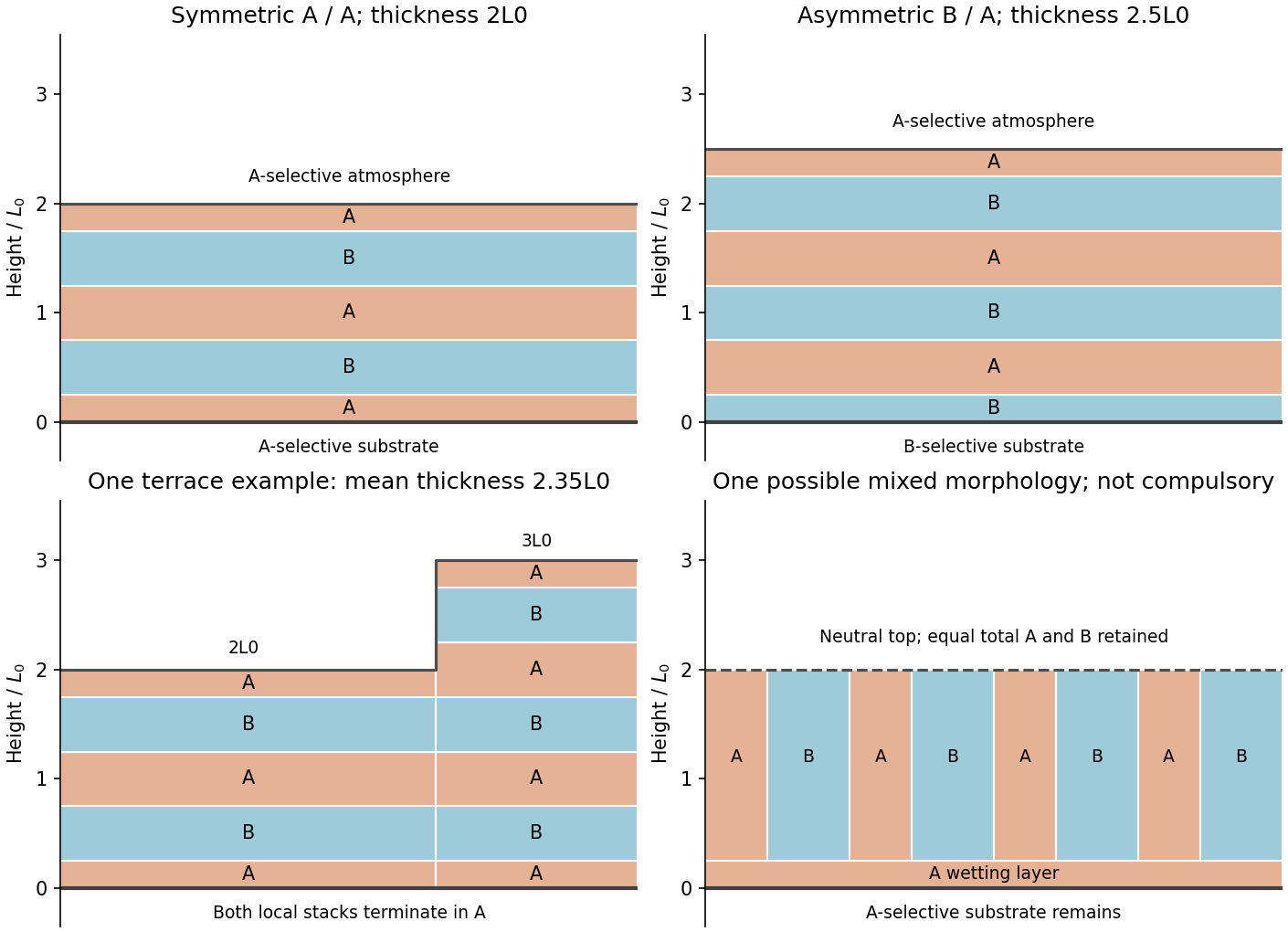
Lamellar terminations, thickness terraces and a single neutral boundary
. Original idealized equal-block diagrams. The neutral-top panel is one admissible mixed arrangement, not a unique prediction; the bottom surface still prefers A. Details.
An asymmetric film with a B-preferring substrate must have an A-preferring atmosphere interface. A parallel stack with half-integer thickness can terminate correctly at both surfaces. For equal block widths, one explicit sequence from bottom to top isThe thicknesses add to , with of each block. B contacts the substrate and A contacts the atmosphere, as shown in the accompanying schematic. The alternating widths in the interior reflect half-period domains, while the terminal domains are half of an interior domain in this idealized construction.
With identical A-selective boundaries, stress-free parallel stacks favour approximately integer multiples of . An arbitrary imposed thickness generally cannot preserve both the bulk period and those terminations everywhere.
A small mismatch can be accommodated by compressing or stretching the lamellae. A larger mismatch can favour terraces, islands or holes with locally commensurate heights, separated by steps of roughly . For example, a mean height can be assembled from regions of heights and , with area fraction at the larger height:The cartoon shows this volume-conserving alternative. Which response wins depends on elastic stretching energy, surface energies, lateral constraints, thickness mismatch and equilibration time. If the substrate and processing permit it, dewetting or a different domain orientation can also occur; an arbitrary thickness does not prove that a single specific terrace pattern must form.
Neutralizing the top boundary removes its preference for A, but the substrate still prefers A. The original integer-period constraint from two A-selective interfaces is therefore relaxed. The film can adjust its top termination without paying the same surface penalty, and thickness frustration can be reduced.
A possible morphology is an A-rich wetting layer near the substrate with lamellae turning towards a more perpendicular arrangement in the upper film, as schematically illustrated. A predominantly parallel stack is also possible if the substrate anchoring and thickness commensurability dominate. Neutrality of the top alone does not uniquely determine the orientation.
If both boundaries were neutral, perpendicular lamellae could expose comparable A and B areas without a selective-surface penalty and would avoid the same parallel-stack thickness constraint. That is a different boundary condition from the one given here. A correct sketch must retain the A preference at the bottom rather than silently replacing it with a second neutral interface.
Positive dielectrophoresis acts up the gradient of the squared RMS field, towards stronger-field regions; negative dielectrophoresis acts down that gradient, towards weaker-field regions. The sign is the sign of .
The force is not generally tangent to an electric field line. Field lines show the direction of the field itself, whereas describes how its strength changes in space. A spatially uniform field gives zero dipole-order dielectrophoretic force even when it is large. Reversing the field each half-cycle does not reverse this time-averaged force, because the relevant intensity-like quantity is quadratic.
At fixed material response, frequency and field-strength gradient,Thus the force is proportional to particle volume. Doubling the radius multiplies the force by eight, not two. This scaling assumes that the particle is small enough for the dipole approximation and does not substantially distort the prescribed field distribution. The mechanical drift speed need not scale with volume, because the hydrodynamic drag also changes with particle size.
For ordinary lossless dielectrics with positive real permittivities,The denominator is positive, soThe particle is more polarizable than the displaced medium and is driven towards the region where its polarization lowers the field-plus-source energy most effectively. If the two permittivities match, this ideal dipole contrast vanishes.
Under the same positive, real-permittivity assumptions,The particle is less polarizable than the surrounding medium and moves towards weaker-field regions. The sign describes the polarizability contrast, not a negative net electric charge. Conducting or lossy media require the real part of the full complex Clausius-Mossotti factor; a comparison of only the real dielectric constants is then insufficient.
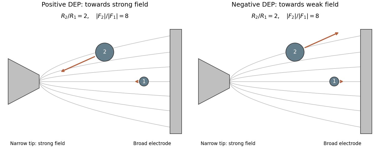
The narrow electrode tip concentrates field lines and produces the strong-field region. For positive dielectrophoresis, both particles move towards that region; for negative dielectrophoresis, both move away. Particle 1 is approximately on the central symmetry line, so its arrow is approximately horizontal. Particle 2 lies above it, so a qualitative gradient arrow points towards or away from the high-field tip rather than simply following its local field line.
The source drawing makes particle 2 approximately twice the radius of particle 1. With the explicitly stipulated equal gradient magnitudes and identical material,Accordingly, the second force arrow should be much longer in either sign case. The exact ratio should remain expressed through the drawn radius ratio because the figure supplies no calibrated particle dimensions. Exact off-axis force directions would require solving the electrode boundary-value problem; the drawing supports a qualitative strong-field/weak-field distinction.

Different materials have different frequency-dependent polarization and conduction. For an convention, a useful relative complex permittivity is . Substituting the particle and medium responses into determines whether each population undergoes positive or negative dielectrophoresis and with what magnitude.
Choose a frequency at which one population has and another has . A nonuniform electrode field then sends them towards different regions, allowing collection in separate channels or trapping one while the other passes. Alternatively, different positive-force magnitudes can produce different deflections in a flowing suspension. A crossover where can selectively suppress the force on one material.
The useful frequency depends on the surrounding medium as well as the particle. An unchanging, real-permittivity model would not by itself give frequency-selective separation; dielectric dispersion or conductivity contrast is needed. Particle size affects force magnitude, and heating, electro-osmotic flow and surface polarization can complicate a real separation.
An Au-containing seed absorbs gallium and forms a liquid Au–Ga alloy under the selected growth conditions. The supplied binary diagram indicates which temperature and Ga fraction lie in the liquid field; alloying allows a liquid catalyst at temperatures far below the melting point of pure Au. Vapour precursors supply Ga and As, which enter or react through the droplet and precipitate GaAs at the liquid–solid interface when the growth chemical potentials make incorporation favourable.
The droplet remains near the wire tip as interface nucleation and step propagation extend the nanowire. Its footprint helps select the wire diameter, though sidewall growth can change the final profile. The catalyst is a reservoir and reaction interface, not a stoichiometric constituent consumed once per GaAs unit.
Low As concentration makes the Au–Ga diagram a useful first approximation to catalyst state, but does not mean that arsenic supply or chemical potential is irrelevant. A binary phase diagram alone cannot calculate supersaturation with respect to ternary GaAs formation, and nanoscale interfacial energies can shift phase boundaries. In situ composition measurements have directly distinguished substantial Ga content from the very small As content of Au-seeded catalyst droplets.[ref]
In situ analysis of catalyst composition during gold catalyzed GaAs nanowire growth by Carina B. Maliakkal and others. 2019, catalyst spectroscopy and comparison with Au–Ga–As phase calculations
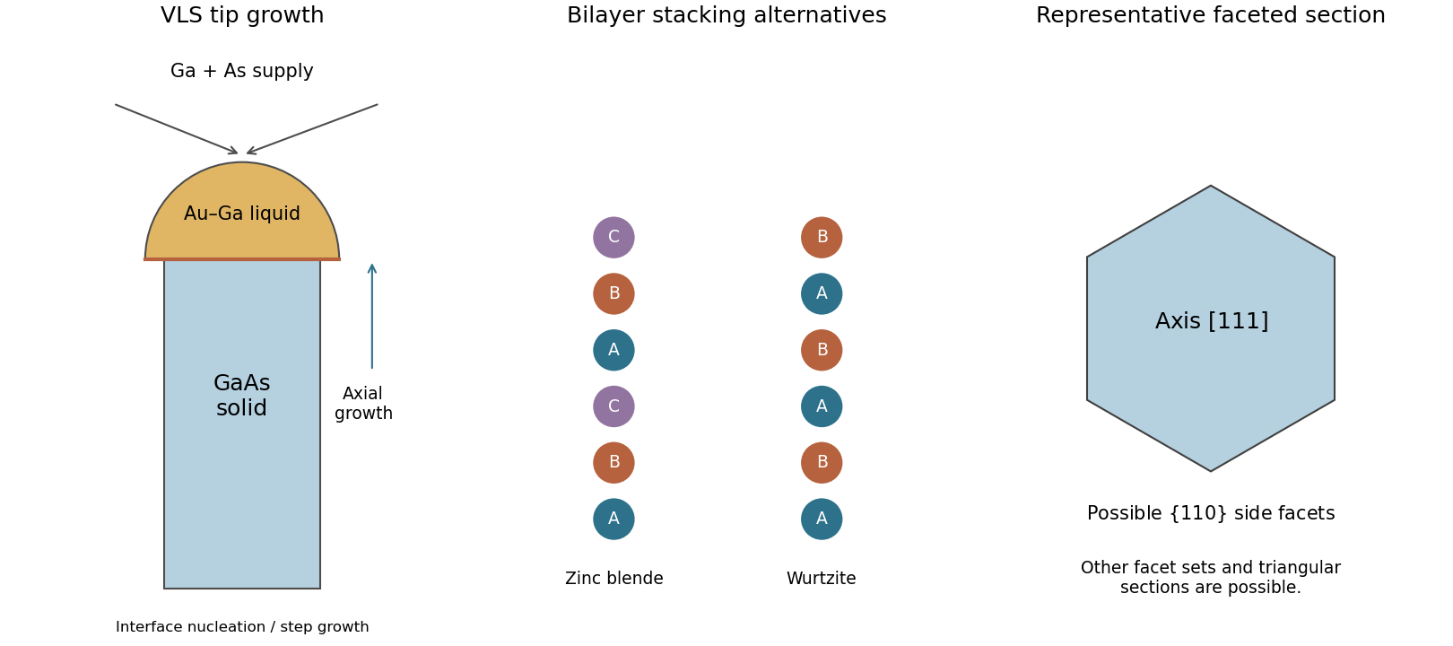

Zinc blende and wurtzite differ in their stacking of tetrahedrally bonded bilayers: an ideal cubic sequence is ABCABC, while the hexagonal sequence is ABAB. During vapor–liquid–solid growth, each new interfacial nucleus can choose between continuing the existing sequence and changing it.
The selected phase can be the one with the smaller nucleation barrier, rather than the lower bulk free energy alone. A nucleus at the droplet–wire–vapour triple line has edge and interfacial energies different from a nucleus fully inside the liquid–solid interface. Schematically, its free energy combines a favourable chemical-potential term with new edge/interface costs and, when appropriate, a stacking penalty. Supersaturation changes the relative importance of these terms; the droplet shape and contact angle change which nucleation sites are available.
Control is therefore possible through temperature, III/V supply ratio, precursor fluxes, catalyst composition, droplet volume/contact angle and wire diameter. Monitoring growth rather than only inspecting cooled specimens helps determine which parameter actually changes the interface. A nucleation model for Au-catalysed III–V wires explicitly showed how triple-line nucleation can favour wurtzite under suitable interface energies and supersaturation.[ref]
Why does wurtzite form in nanowires of III-V zinc blende semiconductors by Frank Glas and others. 2007, competing phase nucleation at the triple line
There is no universal rule that one phase always corresponds to the larger temperature or smaller diameter regardless of catalyst and interface geometry.For the common -axis zinc-blende GaAs wire, a representative cross-section is a faceted hexagon with low-index sidewalls, often described by -type facets. The threefold crystallographic symmetry of a polar direction can make alternate facets inequivalent, so triangular or truncated-triangular sections are also possible. The zinc-blende label alone does not fix a unique hexagon: growth direction, termination, twins, surface chemistry and kinetic facet selection also matter.
The accompanying sketch shows a representative faceted section rather than a circular cylinder. Facets that advance slowly in their normal direction tend to remain exposed, so a kinetic growth shape need not be an equilibrium Wulff shape.
A simple cause of tapering is continued radial vapor–solid growth on sidewalls while the tip grows axially. A lower wire segment has been exposed to precursors for longer than a segment formed near the end of growth. For a roughly constant radial growth speed , its radius gains about , giving a larger base. Substrate-fed species, changing catalyst size and droplet wetting can also contribute. Tapering is not proof that the original VLS droplet was wider at every earlier stage.
Cooling changes the catalyst state that is being measured. Crossing Au–Ga phase boundaries can cause solidification, segregation and intermetallic formation. Solubility changes can expel Ga or precipitate additional GaAs after the intended growth interval. The droplet contact angle and interfacial shape also change as temperature and composition change.
A cooled catalyst–wire interface can consequently have a different composition, phase assemblage, geometry and even last-grown crystal segment from the active growth interface. Continued precursor supply during cooling can add another uncontrolled history. An ex situ observation of a solid catalyst does not prove that growth occurred by a solid-catalyst mechanism, and its final geometry cannot simply be substituted into a nucleation model for the liquid growth stage.
Use in situ microscopy, diffraction or spectroscopy under representative growth conditions, or compare controlled interruption and quench protocols. Quenching reduces some rearrangement but does not guarantee a perfectly frozen interface. The Au-catalysed GaAs composition experiment provides a direct example of measuring catalyst state during growth instead of inferring it from the cooled residue.[ref]
In situ analysis of catalyst composition during gold catalyzed GaAs nanowire growth by Carina B. Maliakkal and others. 2019, motivation for and implementation of in situ catalyst analysis
A c-axis wurtzite ZnO wire has crystallographically polar basal ends, conventionally Zn-terminated and O-terminated , and approximately nonpolar prismatic side facets such as . Crystallographic polarity is not identical to net surface charge in a growth solution: protonation, adsorbates and ionic speciation can change the latter.
For face-selective electrostatic growth inhibition, an oppositely charged additive adsorbs preferentially to a particular face and obstructs incorporation there. Blocking the axial end lowers axial growth relative to radial growth and yields a smaller aspect ratio; blocking sidewalls suppresses radial growth and favours long thin wires.
A primary hydrothermal experiment at pH 11 found negatively charged basal top surfaces and positively charged sidewalls. Positively charged Cd-containing complexes inhibited the top and favoured platelets; negatively charged Al-containing complexes inhibited sidewalls and favoured large aspect ratios. These signs are condition-specific, not fixed by the formal Zn/O termination alone.[ref]
Face-selective electrostatic control of hydrothermal zinc oxide nanowire synthesis by Jaebum Joo and others. 2011, Fig. 1 and pH-dependent complex-ion and surface-charge discussion
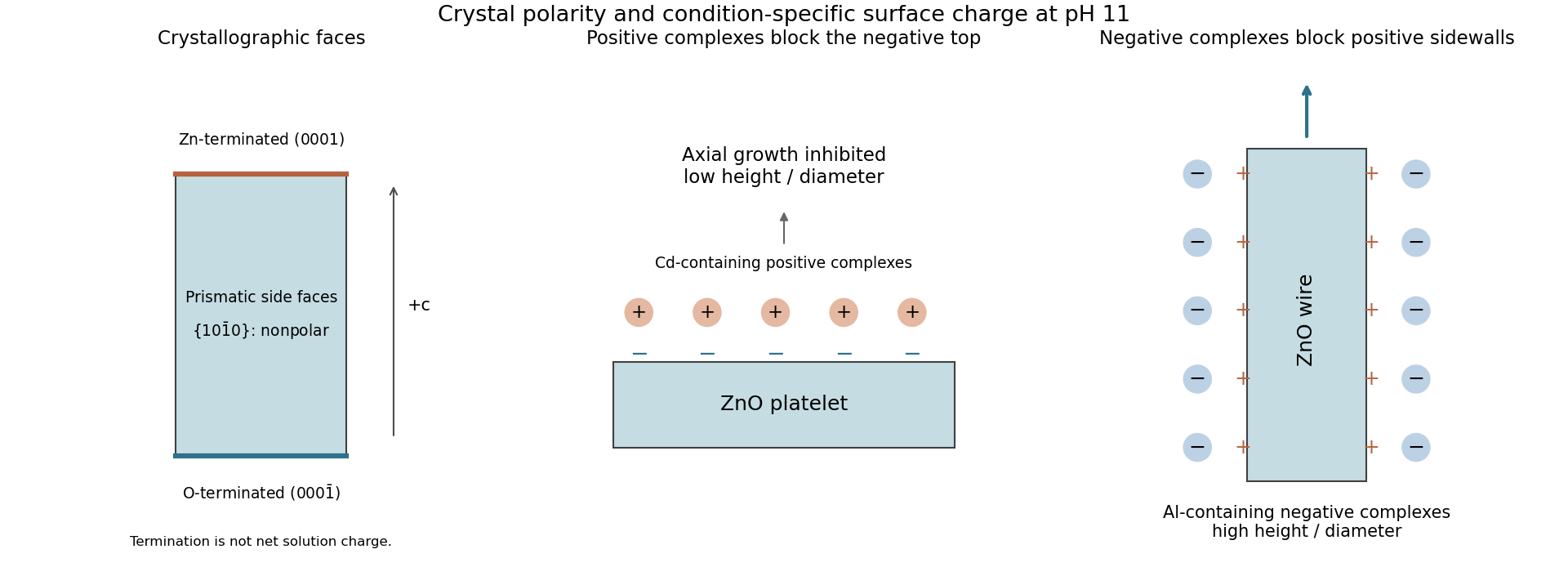
Facet-selective adsorption changes axial and radial ZnO growth
. Original facet-termination diagram and schematic of the cited pH-11 effective surface-charge example. The signs in the adsorption panels denote solution-condition-dependent surface charge, not a universal assignment of charge to crystallographic facets. Details.
One consistent five-postulate formulation is the following; different textbooks group the same content differently.
- State. A pure state is a normalized vector in a complex Hilbert space, with ; vectors differing only by an overall phase represent the same state. For a spinless particle in position representation, is its wavefunction.
- Observables. A physical observable A is represented by a self-adjoint operator . In a Cartesian position representation, and , with .
- Outcomes and probabilities. Allowed ideal measurement outcomes are spectral values of . The Born rule gives , where projects onto the corresponding eigenspace; continuous spectra require the analogous spectral probability measure. The expectation is .
- Ideal measurement update. Conditional on a nonzero-probability outcome , an ideal projective measurement leaves . For a nondegenerate result this is its eigenstate. This is the ideal projection rule, not a description of every general measurement apparatus.
- Time evolution. Between measurements a closed system evolves by the Schrödinger equation, , with Hamiltonian . For time-independent , this gives unitary evolution .
The position-dependent probability density is , and its flux is the probability current. These distinguish the wave amplitude from the measurable particle flow in the following scattering problem.
Place the interface at and let the incident beam travel in the positive x direction. Set the vacuum potential to zero and the solid potential lower by :Equivalently, . The incident kinetic energy is . This ideal potential step assumes a sharp, planar interface, constant particle mass and no absorption, inelastic processes or lateral structure. It models the prescribed decrease in potential without asserting that every real solid has the same electronic interface potential.
For a stationary scattering state, the time-independent Schrödinger equation is . The left side contains the incident and reflected waves, while the solid has no incident wave arriving from positive infinity:Multiplying by gives the time-dependent wavefunctions. The kinetic energy rises inside the lower-potential solid, so and the transmitted wavelength is shorter. A downward step permits a propagating transmitted wave for every , but still generally reflects some incident flux. There is no forbidden region merely because ; the relevant transmitted kinetic energy is .
Classically every particle crosses a downward step and accelerates, so this partial reflection has no classical counterpart. If the step is instead upward to , gives oscillatory transmission with possible reflection, while gives a decaying evanescent wave. A semi-infinite forbidden region carries no transmitted stationary flux; a finite barrier can permit quantum tunnelling to a propagating region beyond it.
For a finite step and equal masses, continuity of the wavefunction and its derivative givesHence the reflected and transmitted amplitude ratios areA travelling wave has probability current , so the flux coefficients areThey satisfy . Using alone as the transmission probability would omit the different transmitted velocity.
For and a downward step of , the transmitted kinetic energy is and . ThereforeThe nonzero reflection is compatible with current conservation even though the potential drops.
Here the step is upward by , so the forbidden-region energy difference is . The bounded wavefunction isThe requested amplitude penetration depth is . Using the supplied mass and ,The probability density decays as , so its depth is half this value. For an ideal lossless semi-infinite step below threshold, the evanescent tail does not imply net stationary particle current deep into the material; the reflected flux is unity.
Scanning tunneling microscopy uses electron tunnelling between a conducting tip and a sample across a narrow vacuum gap. At fixed bias, the strong distance dependence of the current enables sensitive height or electronic-structure measurements; the result depends on local electronic states as well as topography.
A tunnel diode uses tunnelling between occupied and available states across a very thin, heavily doped semiconductor junction. The alignment of those states changes with bias and can produce a region of negative differential resistance, useful in fast switching or oscillation circuits. Both examples require a finite barrier with states available on the other side; an infinitely extended forbidden region is not an equivalent transport geometry.
Articles were limited to the first 100 out of 126 total.
Articles by others on the same topic
There are currently no matching articles.