Write and take , , so the p side is . In the depletion approximation, mobile Electrons and electron holes are negligible compared with the fixed ionized dopants. Their charge density isApplying Poisson equation givesOutside the depletion region, mobile carriers approximately neutralize the dopants, so and . Full dopant ionization alone does not remove the mobile-carrier charge: the result also requires the depletion approximation.
At equilibrium, majority Electrons undergo diffusion from n to p, while majority electron holes diffuse from p to n. Their departure exposes positive donors on the n side and negative acceptors on the p side. The resulting electric field points from n to p and opposes further diffusion. Equilibrium is reached when the chemical potential is constant across the junction. The built-in potential is this electrostatic adjustment, not a discontinuity of the material's band gap.
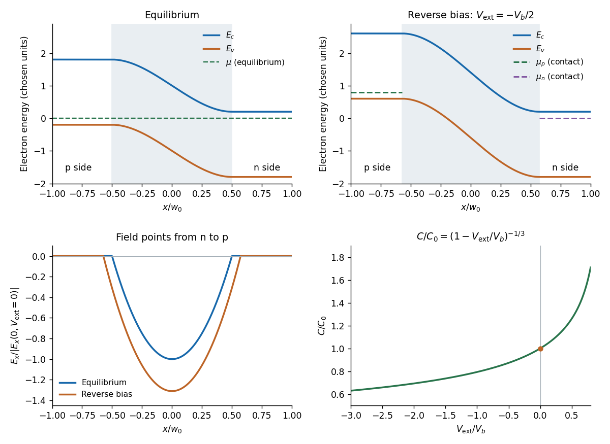
Since electronic band energies shift by , both the conduction band and valence band undergo band bending down from p to n by at zero applied bias. Their separation remains the same gap. In the nondegenerate thermal equilibrium limit the built-in voltage can also be expressed using neutral-edge densities as .
Take the n-contact potential and its electrochemical potential as reference. Applying to the p side changes the total depletion-layer drop toThus is reverse bias: it increases the barrier and widens the depletion region. The bands have horizontal tangents at the neutral edges in this approximation and a smooth cubic bend within the linearly graded layer.
A biased junction is not in global thermal equilibrium. Its contact electron electrochemical potentials obeyUnder reverse bias the p-contact level is higher by . A single horizontal equilibrium chemical potential cannot describe this state; electron and hole quasi-Fermi levels describe the nonequilibrium populations. The sketch marks the contact levels. Detailed spatial quasi-Fermi profiles require transport and recombination information beyond the electrostatic doping profile.

At equilibrium the diffusion currents and drift currents cancel separately for each carrier species. Electron diffusion is from n to p, while the electric field drives electrons from p to n; hole diffusion is from p to n, while hole drift is from n to p. The net current is zero, although these opposing microscopic fluxes are present. In conventional-current signs, both majority diffusion contributions point p to n and the balancing drift contributions point n to p.
Forward bias, , reduces the barrier and enhances majority-carrier diffusion and minority carrier injection. The ideal low-injection Shockley diode equation giveswhere positive current is p to n. For reverse bias, majority diffusion is suppressed and the field sweeps thermally supplied minority carriers across the junction, giving approximately . This saturation is limited by carrier supply rather than a current proportional to the field. Depletion-layer generation, recombination and eventual diode reverse breakdown modify the ideal result.
Let the neutral edges be and and take the exterior electric field to vanish. Integrating between the edges gives , so . This is also the condition of equal and opposite integrated depletion charges.
A second integration with yieldsIt is negative inside the layer, pointing from n to p, and zero at both edges. Its largest magnitude occurs at the metallurgical junction:For reference, choosing gives the cubic electric potential
The electric potential difference is the negative integral of the field:ConsequentlyThe linearly graded junction depletion width has this cube-root dependence because of the linearly growing space charge: the charge on one side scales as , the field as , and its potential integral as . The formula assumes and that the depletion approximation remains applicable.
The positive charge per unit interface area on the n side and negative charge on the p side areUse the signed p-side charge because is the p-side voltage relative to n. Differentiating the width relation givesUsing part (e), the positive junction capacitance per unit area isIt decreases with increasing reverse-bias magnitude as . Equivalently,so a linear versus voltage plot diagnoses this ideal linear grading and can determine .
For this linearly graded junction capacitance, the charge convention matters: if “stored charge” means the positive magnitude , then ; the positive measured capacitance is for . The total net depletion charge is zero and is not the stored terminal charge. At substantial forward bias, minority carrier storage and the failure of the sharp depletion approximation prevent extrapolation of the apparent divergence at .
Articles by others on the same topic
There are currently no matching articles.