For state counting in a Bloch band, take a primitive cubic lattice of spacing and impose periodic boundary conditions on lengths . The allowed wavevectors are . The first Brillouin zone has side , so it contains distinct values in each direction and hence wavevectors. Each orbital-derived energy band has one state per wavevector per spin orientation. ThereforeThe phrase “per atom” attached to in the PDF is a counting error: is the total, not the per-atom count.
By the Pauli exclusion principle, a monovalent crystal supplies valence Electrons and half-fills a spin-degenerate band; its Fermi level lies within allowed states, giving a metal in the independent-electron picture. Two electrons per atom can fill one band. If a band gap separates it from all empty bands, the crystal is a band insulator. An even valence count only permits insulation: overlapping bands can still produce a metal. Conversely, electron interactions can produce a Mott insulator, and symmetry breaking can permit insulation outside this simple spin-degenerate electronic band structure criterion. The relevant count in a crystal with a basis is per primitive unit cell.
In a simple metal, conduction Electrons can move collectively in response to an incident electromagnetic wave. The Drude model gives, with time dependence ,In the low-loss range , the relative permittivity is approximately . The wavevector inside is predominantly imaginary, so the field is evanescent and penetrates only a short distance. Surface currents reradiate the field; little energy enters a good conductor. The normal-incidence Fresnel equations giveMany ordinary metals have their plasma frequency in the ultraviolet, placing visible light below this reflection edge. For the free-carrier contribution permits propagation; at , and . The electrons' inertial response becomes too small to screen the rapidly oscillating field.
Ultraviolet transparency is a simple-metal model prediction, not a universal property of real metals. Electronic transitions between bands and bound-electron absorption can remain strong, shift the plasma edge and prevent transparency; transmission also depends on thickness and attenuation. The robust explanation is the change from a reflective negative-permittivity range to a possible propagating range above the plasma edge.
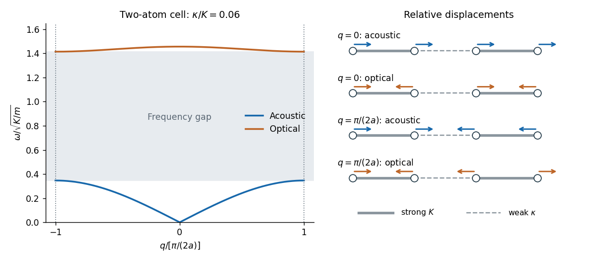
Let adjacent equal masses be separated by , with alternating strong and weak spring constants and , . The pattern repeats after , even though the masses are identical. Thus the first Brillouin zone isChoose the strong bond inside each two-atom primitive unit cell. With displacement amplitudes , the normal mode equations areThe alternating-spring chain dispersion relation is consequentlyThe lower acoustic phonon branch has in-phase motion within the strongly bound pair and . Its small- slope is the speed of sound,The upper optical phonon branch has opposite motion within each pair, with . Here “optical” names the gapped branch; equal neutral masses need not couple to light through an electric dipole.
In the strong-bond limit of the alternating-spring chain, the pairs act almost as rigid dimers in the low-frequency branch, while their internal stretch gives a high, nearly flat branch:At the zone edge the two frequencies are and , separated by a large forbidden frequency interval. Neighbouring cells are out of phase there. Both branches have horizontal tangents at the edge.

For a Hamiltonian with a lattice-periodic potential , its simultaneous energy eigenstates and lattice-translation eigenstates can be chosen in the Bloch wave formEquivalently, . The index labels an energy band; crystal momentum is defined modulo a reciprocal lattice vector. These are the content of Bloch's theorem.
Use one orthonormalized localized atomic orbital at each position . In the nearest-neighbour tight-binding model, translation invariance gives the on-site energy and real hopping integralThe Bloch state isSince , shifting the two summation indices givesThe hopping integral is an energy, and its sign sets whether is a minimum or maximum. is the diagonal matrix element in the crystal Hamiltonian, which can differ from an isolated-atom energy.
The orthogonal tight-binding approximation matters. If raw neighbouring orbitals retain a nonzero orbital overlap in their normalization, projection instead gives a generalized eigenvalue problem and the nonorthogonal nearest-neighbour tight-binding band . The stated cosine band follows after orthonormalization and nearest-neighbour truncation, or after neglecting that overlap metric while retaining the hopping it motivates.
A site in a primitive cubic lattice has six nearest neighbours, at , and . Repeating the Bloch state calculation with equal hopping integrals along all six bonds givesThe cosine sum ranges from to within the first Brillouin zone. ThereforeFor the minimum is at the zone centre; for the maximum is there.
For , expand each cosine to second order:To this order a fixed energy fixes , so the constant-energy surfaces are spheres. The band effective mass tensor satisfiesFor bonding hopping this is a positive electron mass at the band bottom. If , is a maximum with negative electronic mass, or positive electron hole mass . The spherical shape is a quadratic approximation; cubic anisotropy appears in the fourth-order terms.
Taking so that the zone centre is a minimum, the effective mass for exponentially decaying tight-binding hopping isIts logarithmic derivative isThe curve decreases for , has a unique minimum at , and increases for :The formal limits are an divergence as and an exponential divergence as . The small-separation extrapolation eventually invalidates the localized-orbital tight-binding model; the sketch describes the specified formula.
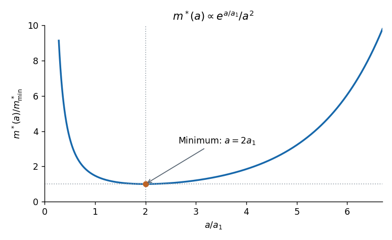
Effective mass versus atomic spacing for exponentially decaying nearest-neighbour hopping
. Original plot of the specified tight-binding model, normalized by its minimum. The minimum occurs at , where the logarithmic derivative of the hopping magnitude balances the explicit band-curvature factor. Details.
The electronic bandwidth is . With reduced from to ,Thus the energy band widens by approximately 1.005 percent, or 1 percent to first order. Compression increases the orbital coupling.
For a degenerate Fermi gas, the Pauli exclusion principle restricts thermally changed occupations to an energy shell of width around the Fermi energy. The number of active Electrons is of order ; each carries an excitation energy of order . Thus the thermal energy grows as and the electronic heat capacity is proportional to .
More precisely, the fixed-particle-number Sommerfeld expansion givesHere is the total spin-summed density of states for the sample. For a three-dimensional parabolic band, , yieldingThe linear law concerns the electronic contribution; the low-temperature lattice heat capacity usually adds a term.
Let and be the carrier density and electronic heat capacity per unit volume. In isotropic kinetic theory, the angular average gives the electronic thermal conductivitywhere is the mean free path associated with the heat-current relaxation time. With ,The Drude model gives the electrical conductivity , where is the momentum relaxation time. ThereforeWhen the same approximately elastic collisions relax heat and charge currents, . Using gives the Wiedemann-Franz law is the Lorenz number. Degenerate electrons move at the Fermi velocity, not the classical thermal velocity; using classical equipartition would give the wrong coefficient.
The Wiedemann-Franz law applies to a normal degenerate metal when the same itinerant Electrons carry heat and charge, scattering is approximately elastic over the thermal shell, and the transport probability varies slowly across the energy interval around the Fermi level. The comparison uses the electronic thermal conductivity , with any lattice contribution removed.
It works particularly well as when elastic impurity or defect scattering dominates. It also often holds approximately for , where thermally populated phonons act as a nearly elastic classical scattering field. Room temperature need not lie above the Debye temperature for every metal.
At intermediate temperatures, inelastic small-angle electron-phonon scattering can relax heat much more efficiently than charge. Then and can be smaller than . Strong energy dependence of scattering, additional neutral heat carriers, or a transition out of the normal metallic state also invalidates the simple derivation. An observed deviation alone does not identify which assumption failed.
For one conduction electron per atom, let be the atom density. State counting in a Bloch band gives the Fermi wavevector . The Debye model preserves the three vibrational modes per atom by a spherical Debye wavevector cutoff , soBoth wavevectors are of order the inverse atomic spacing. The numerical factor uses the spherical Debye approximation; a real zone boundary and the largest-frequency mode depend on direction and branch. Because , short-wavelength acoustic phonons can scatter Fermi surface electrons through substantial angles. For nearly elastic scattering within a spherical Fermi surface,Near room temperature, when a substantial fraction of the phonon spectrum is occupied, electron-phonon scattering is often the main source of electrical resistance. For , the phonon population and scattering rate are approximately proportional to , giving , and roughly constant when the Wiedemann-Franz law holds.
For small-angle electron-phonon transport at low temperature, thermally active acoustic modes instead haveThey predominantly scatter forward. The factor makes such collisions inefficient at relaxing an electrical current, while a phonon energy of order can still substantially change an electron's thermal excitation. Heat-current relaxation therefore need not share the charge-current relaxation time. In the clean three-dimensional acoustic-phonon model this gives but , so the phonon-limited electrical resistivity scales as and . These laws describe the regime before residual elastic scattering takes over; at sufficiently low temperature impurities give nearly constant residual resistivity and , restoring the usual Lorenz number.[ref]
https://home.itp.ac.ru/~grigorev/LectureSlides/MetalsLecture2.pdf. Electron-phonon scattering: distinct low-temperature thermal and electrical transport relaxation rates
Phonons also transport heat themselves, with . At low temperature their population decreases and their phonon mean free path can become boundary- or defect-limited. At higher temperature Umklapp scattering can relax the phonon heat current. Such lattice conduction is an additional contribution, not the quantity constrained by the electronic Wiedemann-Franz law.
Write and take , , so the p side is . In the depletion approximation, mobile Electrons and electron holes are negligible compared with the fixed ionized dopants. Their charge density isApplying Poisson equation givesOutside the depletion region, mobile carriers approximately neutralize the dopants, so and . Full dopant ionization alone does not remove the mobile-carrier charge: the result also requires the depletion approximation.
At equilibrium, majority Electrons undergo diffusion from n to p, while majority electron holes diffuse from p to n. Their departure exposes positive donors on the n side and negative acceptors on the p side. The resulting electric field points from n to p and opposes further diffusion. Equilibrium is reached when the chemical potential is constant across the junction. The built-in potential is this electrostatic adjustment, not a discontinuity of the material's band gap.
Since electronic band energies shift by , both the conduction band and valence band undergo band bending down from p to n by at zero applied bias. Their separation remains the same gap. In the nondegenerate thermal equilibrium limit the built-in voltage can also be expressed using neutral-edge densities as .
Take the n-contact potential and its electrochemical potential as reference. Applying to the p side changes the total depletion-layer drop toThus is reverse bias: it increases the barrier and widens the depletion region. The bands have horizontal tangents at the neutral edges in this approximation and a smooth cubic bend within the linearly graded layer.
A biased junction is not in global thermal equilibrium. Its contact electron electrochemical potentials obeyUnder reverse bias the p-contact level is higher by . A single horizontal equilibrium chemical potential cannot describe this state; electron and hole quasi-Fermi levels describe the nonequilibrium populations. The sketch marks the contact levels. Detailed spatial quasi-Fermi profiles require transport and recombination information beyond the electrostatic doping profile.
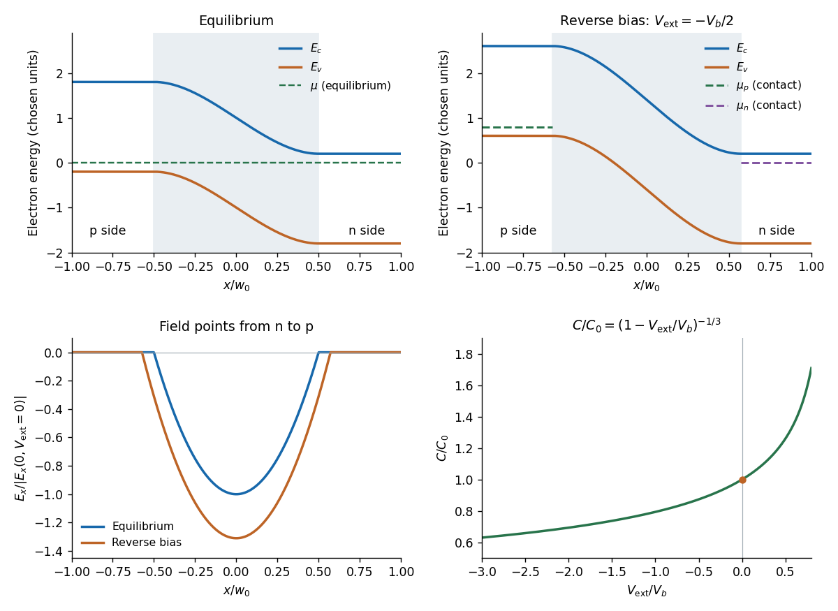

At equilibrium the diffusion currents and drift currents cancel separately for each carrier species. Electron diffusion is from n to p, while the electric field drives electrons from p to n; hole diffusion is from p to n, while hole drift is from n to p. The net current is zero, although these opposing microscopic fluxes are present. In conventional-current signs, both majority diffusion contributions point p to n and the balancing drift contributions point n to p.
Forward bias, , reduces the barrier and enhances majority-carrier diffusion and minority carrier injection. The ideal low-injection Shockley diode equation giveswhere positive current is p to n. For reverse bias, majority diffusion is suppressed and the field sweeps thermally supplied minority carriers across the junction, giving approximately . This saturation is limited by carrier supply rather than a current proportional to the field. Depletion-layer generation, recombination and eventual diode reverse breakdown modify the ideal result.
Let the neutral edges be and and take the exterior electric field to vanish. Integrating between the edges gives , so . This is also the condition of equal and opposite integrated depletion charges.
A second integration with yieldsIt is negative inside the layer, pointing from n to p, and zero at both edges. Its largest magnitude occurs at the metallurgical junction:For reference, choosing gives the cubic electric potential
The electric potential difference is the negative integral of the field:ConsequentlyThe linearly graded junction depletion width has this cube-root dependence because of the linearly growing space charge: the charge on one side scales as , the field as , and its potential integral as . The formula assumes and that the depletion approximation remains applicable.
The positive charge per unit interface area on the n side and negative charge on the p side areUse the signed p-side charge because is the p-side voltage relative to n. Differentiating the width relation givesUsing part (e), the positive junction capacitance per unit area isIt decreases with increasing reverse-bias magnitude as . Equivalently,so a linear versus voltage plot diagnoses this ideal linear grading and can determine .
For this linearly graded junction capacitance, the charge convention matters: if “stored charge” means the positive magnitude , then ; the positive measured capacitance is for . The total net depletion charge is zero and is not the stored terminal charge. At substantial forward bias, minority carrier storage and the failure of the sharp depletion approximation prevent extrapolation of the apparent divergence at .
Articles by others on the same topic
There are currently no matching articles.