Solution
ID: past-exam-of-the-physics-a-course-of-the-university-of-cambridge/2018/paper-2/section-d/d12/solution
Past exam of the physics A course of the University of Cambridge 2018 Paper 2 Section D D12 Solution by  Codex 0 2026-10-18
Codex 0 2026-10-18Doping changes the mobile carrier population by introducing controlled impurity levels. In an intrinsic semiconductor, the filled valence band is separated from the nearly empty conduction band by a band gap . Thermal excitation produces an electron-hole pair, so the Electron and hole number densities obey . A electron hole represents a missing valence-band Electron and behaves as a mobile positive charge carrier. For nondegenerate bands in thermal equilibrium,Here are the effective density of states, the band edges, and denotes the chemical potential, conventionally called the Fermi level. The semiconductor mass-action law holds in this nondegenerate equilibrium regime.
In a tetrahedrally bonded elemental semiconductor such as silicon, a substitutional group-V atom has an extra outer Electron relative to the host. It is a donor impurity: a shallow level just below can ionise, releasing an Electron to the conduction band and leaving a fixed positively charged donor. The resulting n-type semiconductor has Electrons as majority carriers and holes as minority carriers. Conversely a group-III substitution supplies one fewer bonding Electron. An acceptor impurity can take an Electron from the valence band, leaving a mobile electron hole and a fixed negative acceptor; the resulting p-type semiconductor has holes as majority carriers.
The impurity state is shallow because the Electron or hole responds to a screened Coulomb potential and an effective mass, rather than the bare atomic potential. A simple hydrogenic donor estimate iswhere is the relative permittivity. This is a useful scaling model, with real band anisotropy and central-cell effects omitted. Dopants are fixed in the lattice; their ionisation changes mobile carrier numbers without making a uniformly doped bulk sample carry a large net electric charge.
The charge neutrality condition isWhen shallow dopants are almost fully ionised and , an n-type region has and . A p-type region similarly has and . Thus compensation by the opposite impurity type reduces the majority-carrier density; the total dopant concentration is not generally the mobile carrier density. At sufficiently high impurity density the degenerate semiconductor regime requires the full Fermi-Dirac distribution and these exponential approximations fail.
There are three useful temperature regimes. At low temperature, dopant freeze-out leaves many shallow levels un-ionised. In the extrinsic regime, the dopants are largely ionised and set the majority-carrier density. At high enough temperature, intrinsic pair creation dominates and approach . The Fermi level moves towards the conduction band with donor doping and towards the valence band with acceptor doping. The electrical conductivity isDoping therefore controls conductivity and its carrier type, but ionised impurities also scatter carriers and can reduce charge carrier mobility. Carrier density and mobility must both be considered.
A p-n junction forms when p-type and n-type regions are joined within a semiconductor. Initially the concentration gradients drive diffusion current: Electrons diffuse from the n region to the p region and holes in the opposite direction. Recombination removes mobile majority carriers near the join, exposing fixed positive donors on the n side and fixed negative acceptors on the p side. This forms a depletion region and an electric field directed from n to p. Its drift current opposes diffusion. At equilibrium the net current vanishes and the Fermi level is uniform, although the band edges vary spatially through band bending.
For an abrupt nondegenerate junction with fully ionised dopants, its built-in potential isUnder the depletion approximation, the space-charge densities are on a p-side width and on an n-side width . Integrating Poisson equation and imposing zero field outside gives andMost of the depletion width therefore extends into the more lightly doped side. The schematic shows the impurity levels before contact and the resulting space charge and potential after contact; there is no externally extractable equilibrium battery voltage from the built-in field alone.
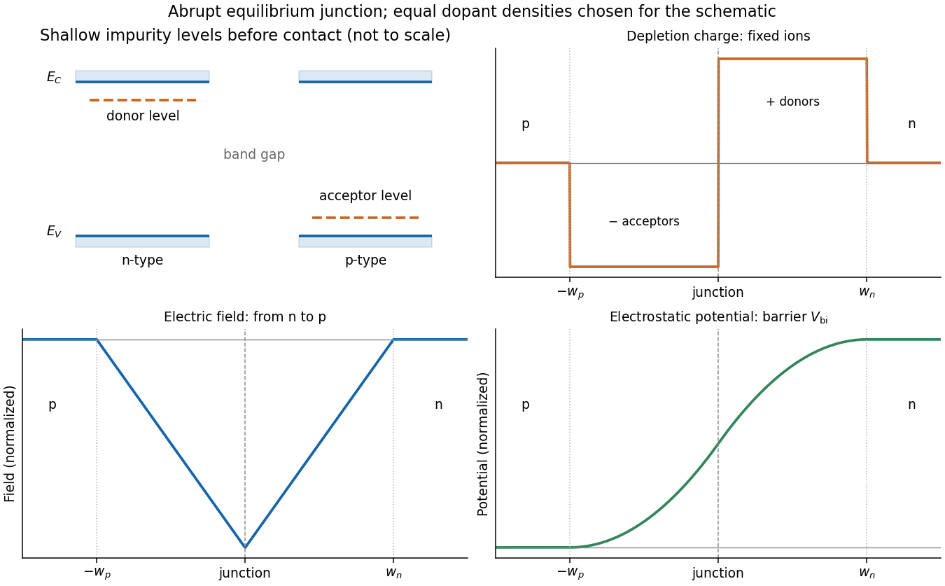
Shallow donor and acceptor levels, and charge, field and potential in an equilibrium abrupt p-n junction
. Details. 
A forward bias, with p positive relative to n, reduces the barrier from towards and injects minority carriers across the junction. In the ideal low-injection, diffusion-controlled regime this produces the Shockley diode equation, . Reverse bias increases the barrier and the depletion region; only a small thermally generated minority-carrier current flows before breakdown. Reverse-biased depletion regions also give a voltage-dependent junction capacitance. Real devices have recombination, leakage, series resistance and breakdown mechanisms beyond the ideal law. Controlled doping creates majority and minority carriers, and their junction produces a depletion barrier that makes rectification possible.
New to topics? Read the docs here!