An intrinsic semiconductor has thermally generated conduction electrons and valence holes, with at equilibrium in the ideal undoped neutral material. Their abundance is controlled by its band gap, temperature and band density of states.
An extrinsic semiconductor has its mobile carrier populations substantially modified by electrically active impurities. A donor impurity can supply electrons, producing n-type material; an acceptor impurity can capture a valence electron and leave a mobile electron hole, producing p-type material. Compensation and incomplete ionization can modify these simple counts. At low temperature dopant freeze-out can occur; at sufficiently high temperature intrinsic pair production can overwhelm a fixed dopant density. Doping and the dominant transport regime are related but are not interchangeable descriptions at every temperature.
Assume nondegenerate three-dimensional parabolic band edges, a fixed gap and approximately temperature-independent density-of-states effective masses. Let be the chemical potential, and the band edges, and their effective density of states. Boltzmann occupation givesFor one spin-degenerate spherical conduction extremum, direct integration of givesand similarly for the valence band with its appropriate density-of-states mass. Valley and additional band degeneracies can be included in these prefactors. The factor follows from the integral .
Multiplication removes the chemical potential:The semiconductor mass-action law combined with intrinsic charge neutrality, , therefore givesThe intrinsic chemical potential is not necessarily exactly midgap: . Equal effective masses are unnecessary for the displayed carrier-density law. A changing gap, effective mass or degeneracy would make the prefactor or activation law temperature dependent.
Choose longitudinal current along , magnetic field along , and define the oriented Hall coefficient by . For one carrier type with signed charge , a stationary transverse force balance is . Since , this gives . Using ,This is the weak-field isotropic one-carrier approximation with Hall scattering factor one, not a general multiband identity.
Under the stipulated electron-dominated approximation, the given Hall magnitudes implyTake the ratio of the intrinsic activation law:Solving gives the model's activation-gap estimateThis result uses the supplied Hall-temperature ratio and the fixed-gap, fixed-prefactor assumptions. A temperature-dependent gap or changing Hall factors would modify its interpretation.
The source's description of electrons as intrinsic silicon's majority carriers needs qualification. Intrinsic neutrality gives equal electron and hole concentrations, not an electron density majority. Electrons can nevertheless dominate conductivity and the Hall response because their mobility is larger. For two weak-field carriers,At this becomes . Thus explains the negative sign, while the one-electron formula is quantitatively accurate only if the hole contribution can be neglected. Equality itself is a concrete counterexample to a literal electron-number-majority claim. The numerical deductions above retain the approximation explicitly requested by the source.
The sign must become positive, so use p-type acceptor impurities, such as boron substituting for tetravalent silicon. Assume uncompensated, fully ionized acceptors of density , nondegenerate carriers and equilibrium throughout the interval. Charge neutrality and mass action giveFor a nearly constant hole-dominated Hall coefficient, the dopant plateau must persist up to the highest temperature. Its necessary concentration scale is thereforeThe order-of-magnitude onset is , but equality is not a flat plateau: at , , changing the hole-only Hall coefficient by about 38 percent. The word approximately does not define a unique sharp minimum without a tolerance.
For , , so the hole-only varies by a fraction of order . An illustrative one-percent tolerance in that approximation is obtained with . This gives and less than one percent hole-density-induced variation. It is an explicit plateau criterion, not an exact minimum deduced from the unspecified word approximately.
At 300 K the minority electron concentration isThus the onset-scale estimate gives about , whereas the explicit ten-times-larger plateau choice gives .
The acceptor density for a stable Hall sign can be more restrictive if both carriers matter. With mobility ratio , positive Hall sign requires , or . In the strongly extrinsic limit the full two-carrier Hall correction scales as , not just . Hence a true measured-Hall tolerance can require a larger dopant density than the hole-only illustration. Mobilities and their temperature dependence are not supplied, so they cannot be used to manufacture a unique sharper minimum.
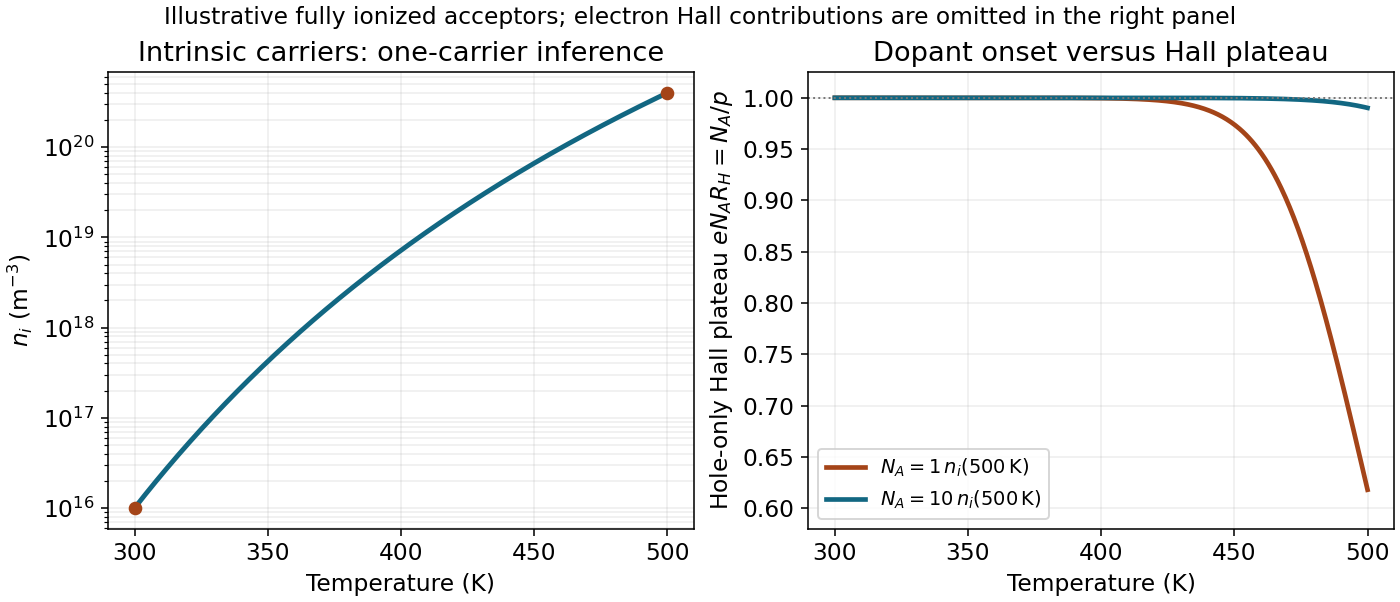
Intrinsic carrier activation and the hole-only Hall plateau for two explicitly chosen acceptor densities; concentrations are model estimates, not extra measurements
. Details. 
Articles by others on the same topic
There are currently no matching articles.