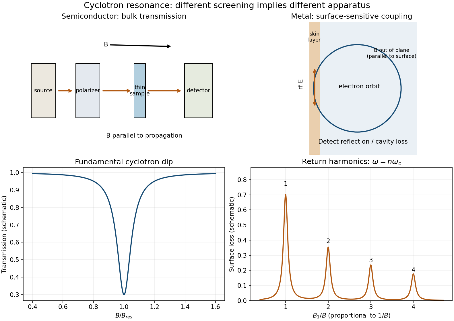
In a low-carrier-density semiconductor use a thin, cold sample in a transmission spectrometer. Direct microwave or far-infrared radiation through it, commonly with propagation parallel to and electric field transverse to it. Sweep at fixed frequency and detect transmitted power. The active circular polarization shows an absorption peak, or transmission dip, near . Resolving it requires a long enough scattering time, .
A metal's large plasma frequency usually prevents that radiation from sampling its bulk directly. In surface cyclotron resonance in a metal, put approximately parallel to a clean metal surface and excite an rf electric field in the skin depth, transverse to . Electron orbits extend into the bulk and repeatedly return to that layer. Coherent energy absorption occurs when the rf phase repeats on a return, including harmonics . Measure cavity loss, reflected power, or surface impedance rather than attempting ordinary bulk transmission. The characteristic regime has cyclotron radius larger than the skin depth and sufficiently specular, long-lived orbits.
For the spherical parabolic band the metal harmonic fields areThey are evenly spaced in , with amplitudes and widths determined by surface geometry and scattering. A semiconductor generally gives the simple bulk fundamental, whereas the metal can show this harmonic series in a surface-loss signal. For an anisotropic real Fermi surface the measured mass is the appropriate cyclotron effective mass rather than necessarily every component of a transport effective-mass tensor. These classical resonance harmonics are distinct from the Landau-level quantum oscillations in c.

Articles by others on the same topic
There are currently no matching articles.