A common implementation uses a gallium arsenide/aluminium gallium arsenide heterostructure with a two-dimensional electron gas near the interface. electrons supplied by remote donors occupy quantized normal-direction states, while an undoped spacer reduces ionized-impurity scattering. Surface metallic gates, insulated from the conducting layer, deplete selected regions when negatively biased.
Leave a small conducting island bounded by depleted regions and connect it weakly to source and drain reservoirs through two tunable constrictions. A plunger gate controls the island potential/population; barrier gates control tunnel coupling. Ohmic contacts connect the reservoirs to the measurement circuit. Vertical heterostructure confinement plus lateral depletion force defines the dot. A 2DEG without lateral gates would remain extended in its plane.
The original device diagram labels the gates, island, tunnel barriers and reservoirs. Charge stability and spectroscopy versus gate/bias should verify that an isolated weakly coupled island has actually formed; a lithographic outline alone is insufficient.
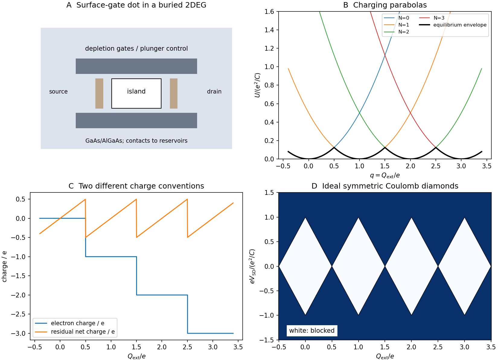
Gate-defined dot, charging parabolas, charge steps and Coulomb diamonds
. Original schematic and constant-capacitance model plots. The conductance map is an idealized symmetric-bias cartoon, not experimental data or a microscopic tunnelling calculation. Details.
Let be the island's total electrostatic capacitance and the charge offset induced by gates, reservoir potentials and fixed background charges. In the constant-capacitance model,Taking the difference givesChanging gate voltage changes approximately linearly, for example through .
For fixed , is a parabola. At small temperature/bias, the preferred integer is the one nearest ; the equilibrium energy follows the lower envelope of these parabolas. Adjacent charge states become degenerate at , allowing small-bias sequential current when the two barriers are transmissive.
The excess-electron charge is a staircase. If “net charge” includes the induced compensating charge, define ; that residual charge is a sawtooth between and in equilibrium. The opposite sign convention reverses the sawtooth. State the charge convention: an integer electron-charge staircase and a residual electrostatic-charge sawtooth describe different quantities.
A larger source–drain bias opens an energy window between reservoir electrochemical potentials. When a charge-addition/removal transition enters that window, sequential tunnelling becomes allowed even away from a zero-bias degeneracy. The low-conductance regions in a gate/bias map are Coulomb diamonds.
For an illustrative symmetric device with reservoir potentials , let and . In the charge- interval, the classical blockade domain isIt shrinks to zero at . Unequal capacitances change edge slopes and voltage division; the figure's symmetry is a chosen model, not a universal device property.
Quantum confinement adds discrete single-particle levels and spin structure. In a constant-interaction approximation, successive addition energies contain plus the relevant orbital spacing, so diamond sizes need not all match. Excited-state tunnelling can produce extra conductance lines. At stronger coupling, cotunnelling and charge fluctuations can give leakage beyond a simple sequential classical model. Thus temperature and coupling must be small enough to resolve the charging and level structure separately.
An initially localized escaping electron occupies a superposition of lead momentum states. In a uniform free one-dimensional lead,A packet centered at moves with group velocity and generally spreads because its components have different velocities. For an initially unchirped minimum-uncertainty Gaussian wave packet,This illustrates dispersive evolution; the actual emission contact determines and whether only outward-propagating components are appreciable. It does not instantaneously become a single lead plane wave.
A single-electron transistor used as a sensitive electrometer exploits Coulomb blockade: a nearby charge shifts the offset and therefore the conductance peaks. This requires stable calibrated capacitances and low charge noise, rather than merely a small conductor.
Articles by others on the same topic
There are currently no matching articles.