The left transistor is an n-channel MOSFET in a p-type silicon substrate; the right is a p-channel MOSFET in an n-well. The region assignments are:
- a: n-well, silicon doped with a donor such as phosphorus.
- b: p+ substrate contact, heavily boron-doped silicon.
- c: n+ source of the nMOS device, arsenic- or phosphorus-doped silicon.
- d: n+ drain of the nMOS device, with the same donor dopants.
- e: p+ drain of the pMOS device, boron-doped silicon.
- f: p+ source of the pMOS device, boron-doped silicon.
- g: n+ well contact, heavily donor-doped silicon.
- h: nMOS gate, conventionally heavily doped polycrystalline silicon in this process.
- i: thin nMOS gate dielectric, conventionally silicon dioxide.
- j: pMOS gate, conventionally heavily doped polycrystalline silicon.
- k: thin pMOS gate dielectric, conventionally silicon dioxide.
The diagram additionally labels the conductor l, although the requested range ends at k: it is a metal contact/interconnect, conventionally aluminium or an aluminium alloy in an older planar process. Modern processes can use metal gates, high-permittivity gate dielectrics and different interconnect stacks; these are alternatives, not evidence that the illustrated conventional gate is aluminium.
For a CMOS inverter, join h and j to the input and d and e to the output. Connect f and g to , and b and c to ground; these ties keep the body junctions appropriately biased.
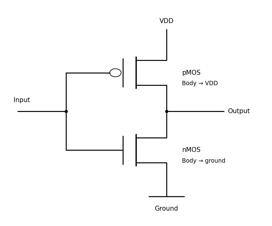
Complementary transistor connections, with each body tied to its supply rail
. Source. Details. 
Articles by others on the same topic
There are currently no matching articles.