The left transistor is an n-channel MOSFET in a p-type silicon substrate; the right is a p-channel MOSFET in an n-well. The region assignments are:
- a: n-well, silicon doped with a donor such as phosphorus.
- b: p+ substrate contact, heavily boron-doped silicon.
- c: n+ source of the nMOS device, arsenic- or phosphorus-doped silicon.
- d: n+ drain of the nMOS device, with the same donor dopants.
- e: p+ drain of the pMOS device, boron-doped silicon.
- f: p+ source of the pMOS device, boron-doped silicon.
- g: n+ well contact, heavily donor-doped silicon.
- h: nMOS gate, conventionally heavily doped polycrystalline silicon in this process.
- i: thin nMOS gate dielectric, conventionally silicon dioxide.
- j: pMOS gate, conventionally heavily doped polycrystalline silicon.
- k: thin pMOS gate dielectric, conventionally silicon dioxide.
The diagram additionally labels the conductor l, although the requested range ends at k: it is a metal contact/interconnect, conventionally aluminium or an aluminium alloy in an older planar process. Modern processes can use metal gates, high-permittivity gate dielectrics and different interconnect stacks; these are alternatives, not evidence that the illustrated conventional gate is aluminium.
For a CMOS inverter, join h and j to the input and d and e to the output. Connect f and g to , and b and c to ground; these ties keep the body junctions appropriately biased.
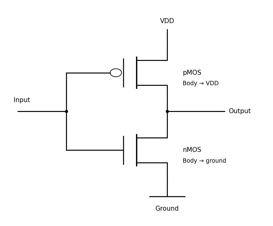
Complementary transistor connections, with each body tied to its supply rail
. Source. Details. 
A MOSFET is a voltage-controlled three-terminal switch: the insulated gate controls a conductive channel, giving high input impedance and useful current gain at the circuit level. A CMOS inverter actively restores either logic rail, has voltage gain near its switching threshold, and ideally draws no static supply current in either settled logic state. Real devices have leakage and consume energy while switching.
A single p-n junction is a two-terminal diode; its current is controlled by its own terminal voltage, so it does not by itself provide an independently controlled switch, gain and restoring inversion. Cross-coupled CMOS inverters form a bistable memory element. A lone inverter is not itself a complete memory cell, and a p-n junction can still serve useful rectification or capacitance functions.
Start with a lightly boron-doped p-type Si wafer. Define an implantation opening for the pMOS region using an oxide/nitride implantation mask, then implant donor ions, commonly phosphorus, at energies and doses giving the required well depth and concentration. An anneal activates donors and repairs damage; thermal drive-in can deepen and smooth the well profile. The donor concentration must exceed the original acceptor concentration in the well. Retain p-type material outside it for the nMOS device. Form a later n+ well contact to tie the n-well to the positive supply; the p+ substrate contact ties the substrate to ground. Diffusion from a donor source is an alternative to ion implantation and drive-in.
Clean the exposed silicon and grow a thin, high-quality SiO2 gate dielectric by controlled dry thermal oxidation. Deposit polycrystalline silicon, conventionally by low-pressure chemical vapour deposition from silane, dope it in situ or by subsequent implantation and activation, and pattern/etch it to define the two gates. Phosphorus or arsenic gives n+ polysilicon; boron gives p+ polysilicon where the selected gate-work-function process requires it. A traditional single-poly process may use a common gate doping instead; gate and source/drain doping need not be identical.
The patterned gates subsequently serve as self-alignment masks for donor-doped nMOS source/drain and acceptor-doped pMOS source/drain regions. Annealing activates these dopants. Keep the oxide thin and uniform enough for strong electrostatic control but free from pinholes and excessive leakage. A high-permittivity dielectric deposited by atomic layer deposition with a metal gate is a modern alternative, rather than the conventional polysilicon/SiO2 stack drawn.
Articles by others on the same topic
There are currently no matching articles.