Two layers need not have the same electronic structure everywhere. Different rotational alignments create domains of twisted bilayer graphene; AB-stacked regions instead have the usual coupled low-energy bilayer bands. In a twisted domain, displaced Dirac cones hybridize where they meet, producing avoided crossings and saddle points in the two-dimensional dispersion relation. The resulting Van Hove singularities enhance optical transitions at energies that depend on the twist angle. Different domains therefore absorb different parts of the visible spectrum and can show different colours despite having the same layer count.[ref]
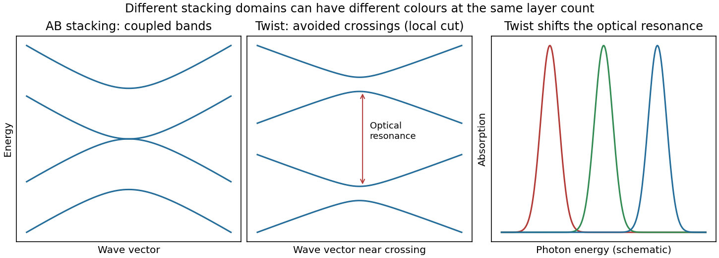
Bilayer stacking changes the bands and optical absorption
. Original illustrative bands: AB-stacked bands, a local cut through avoided crossings in a twisted domain, and schematic angle-dependent absorption peaks. The middle panel is a local cut, not the entire two-dimensional band structure. Source. Details.
On a silicon/silicon-dioxide substrate, reflected beams from the film stack also interfere. The wavelength-dependent optical response of the bilayer graphene changes this reflected contrast, making the domain differences visible. The observation is consistent with stacking domains; colour alone does not uniquely prove a twist angle. Variations in oxide thickness, trapped contamination, folds or local doping can also change contrast and should be checked independently, for example by Raman spectroscopy.
The gas impingement flux onto a surface follows from the normal component of the Maxwell-Boltzmann distribution:Here and , givingAssume a conventional monolayer density and unit sticking coefficient. The incident-monolayer time isThus a few milliseconds is the usual contamination-time estimate at this pressure.
The assumed molecular footprint matters: neither nor the sticking coefficient is specified. More generally if the sticking probability is and desorption is negligible. Water can desorb rapidly from clean graphene at room temperature, so the incident-monolayer estimate does not establish that a stable, complete water layer actually forms in that time. Residues and defects can increase local adsorption.
An atomic layer deposition recipe depends on the surface chemistry during the first cycles. A silicon wafer normally carries native oxide with reactive hydroxyl groups. A pristine graphene basal plane has no comparable dense population of dangling bonds or hydroxyl groups, so precursor adsorption and initial nucleation are much less uniform.
Consequently the nominal number of cycles calibrated to give on silicon can instead give isolated alumina islands, preferential decoration of edges, grain boundaries and defects, and uncovered graphene between islands. Adsorbed transfer residues may provide additional, irregular nucleation sites. Once alumina has nucleated, later cycles grow on the alumina normally; the problem is delayed, spatially uneven nucleation. The resulting local island height can exceed the film's area-averaged equivalent thickness.[ref]
Atomic layer deposition of metal oxides on pristine and functionalized graphene by Xinran Wang and others. Pristine graphene nucleation at edges and defects, and uniform growth after noncovalent functionalization
Two suitable improvements are:
- Introduce a dense, controlled nucleation layer, for example a noncovalently adsorbed functional layer carrying reactive groups or a very thin oxidized metal seed. This supplies precursor-binding sites while limiting damage to the conducting carbon network.
- Optimize initial exposure rather than reuse the silicon recipe unchanged: use longer precursor residence/soak times and suitably reduced initial temperature to increase adsorption and nucleation, then continue normal cycles after closure. Direct sub- continuous growth with extended residence times has been demonstrated.[ref]Parameter space of atomic layer deposition of ultrathin oxides on graphene by Adrianus I. Aria and others. Pulse/residence-time control of initial nucleation and continuous ultrathin films
Ozone or a mild plasma is another possible activation route, but it must be controlled because creating covalent defects can degrade the electrical properties that motivate using graphene.
Articles by others on the same topic
There are currently no matching articles.