A single-walled carbon nanotube confines the electron around its circumference while allowing motion along its axis. Nanotube zone folding therefore turns the graphene bands into one-dimensional subbands. A semiconducting carbon nanotube has no allowed circumferential wave vector through a Dirac valley; a metallic tube has a band crossing at the Fermi energy in the ideal model. Each massive subband edge gives a one-dimensional van Hove singularity in the density of states, and corresponding peaks appear in the joint density of states.
For light polarized along the tube, the main electric-dipole selection rule conserves circumferential angular momentum: transitions connect matching valence and conduction subbands. These finite-energy transitions are conventionally in a semiconducting carbon nanotube and in a metallic tube. A metallic band crossing does not make its first strong interband peak have zero energy. Perpendicular polarization admits different angular-momentum channels, often much weaker because of depolarization. Excitons, dielectric screening and trigonal warping modify the simple band-edge transition energies.
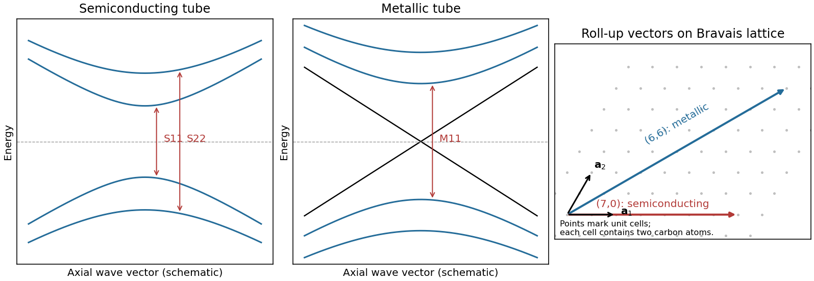
Nanotube optical transitions and two example roll-up vectors
. Original band and lattice schematics. Arrows indicate matching-subband transitions; the metallic crossing is separate from its finite-energy interband resonance. Lattice points represent graphene unit cells rather than individual atoms. Source. Details.
Experimentally, measure absorption versus photon energy; Raman spectroscopy becomes resonantly enhanced when the excitation matches an optical transition. A photoluminescence excitation spectrum of dispersed semiconducting tubes correlates excitation near with emission near after relaxation. Metallic tubes generally lack comparable bright emission because nonradiative relaxation is efficient. Combining optical energies with radial-breathing-mode Raman spectroscopy or electron diffraction assigns tube diameter and roll-up indices; a Kataura plot organizes those assignments.[ref]
Structure-assigned optical spectra of single-walled carbon nanotubes by Sergei M. Bachilo and others. Excitation-emission spectroscopy and assignments to nanotube structures
Let be equal-length primitive translation vectors of the graphene lattice, separated by . The carbon nanotube chiral vectoridentifies the two points joined when the sheet is rolled: is the circumference, not the tube axis. The right-hand panel of the preceding original diagram shows and .
The periodic boundary condition is , with an integer. Applying it at either Dirac valley gives the nanotube zone folding criterionfor a metallic tube. Thus is an armchair metallic example, whereas is a zigzag semiconducting example. Other choices with also give a semiconducting carbon nanotube.
This criterion is the ideal flat-sheet approximation. Curvature can open a small gap in nominally metallic non-armchair tubes; ideal armchair tubes remain gapless in that approximation. The property is determined by the wrapping vector, not simply by calling a tube “chiral” or by its diameter alone.
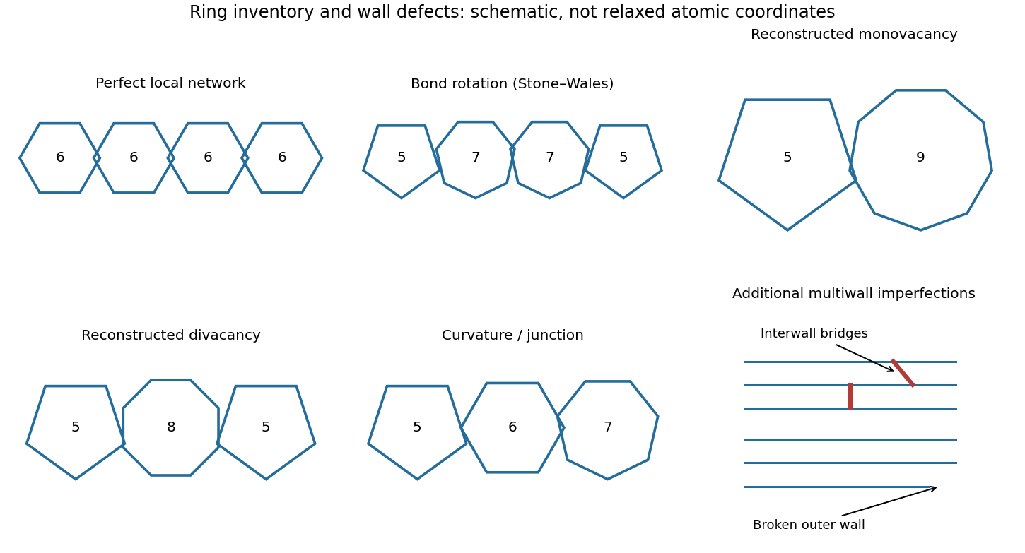
The important distinctions are changes of ring topology, missing or added atoms, and changes of local bonding:
- A Stone-Wales defect rotates one carbon-carbon bond by approximately , converting four hexagons into a --- ring arrangement without adding or removing atoms. It changes strain and electronic scattering.
- A carbon nanotube vacancy defect removes an atom. Reconstruction commonly gives a pentagon and a nine-membered ring, with an undercoordinated site; a reconstructed divacancy can give a -- arrangement. Larger vacancies make holes or broken walls.
- An adjacent pentagon-heptagon pair acts as a dislocation in the hexagonal network. It can connect regions with different wrapping indices, producing a bend or an electronic junction. Isolated nonhexagonal rings impose curvature: pentagons favor positive curvature and heptagons negative curvature.
- An interstitial defect, an adsorbed atom, or chemical functionalization can distort the network and locally change bonding toward . These defects can scatter carriers and create chemically reactive sites.

Closed end caps require nonhexagonal rings, typically six pentagons per hemispherical cap; these are part of the cap topology rather than necessarily damage. Kinks, buckling, branches and incomplete closure are larger-scale structural imperfections.
A multi-walled carbon nanotube can contain any of these defects in individual shells, plus interrupted or terminated shells, extra incomplete graphitic layers, irregular interwall spacing, and covalent interwall bridges formed by displaced atoms. Such bridges change intershell coupling and sliding. Different shells having different wrapping indices is normal and is not, by itself, a defect.
Two layers need not have the same electronic structure everywhere. Different rotational alignments create domains of twisted bilayer graphene; AB-stacked regions instead have the usual coupled low-energy bilayer bands. In a twisted domain, displaced Dirac cones hybridize where they meet, producing avoided crossings and saddle points in the two-dimensional dispersion relation. The resulting Van Hove singularities enhance optical transitions at energies that depend on the twist angle. Different domains therefore absorb different parts of the visible spectrum and can show different colours despite having the same layer count.[ref]
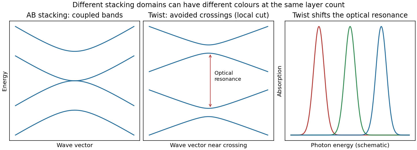
Bilayer stacking changes the bands and optical absorption
. Original illustrative bands: AB-stacked bands, a local cut through avoided crossings in a twisted domain, and schematic angle-dependent absorption peaks. The middle panel is a local cut, not the entire two-dimensional band structure. Source. Details.
On a silicon/silicon-dioxide substrate, reflected beams from the film stack also interfere. The wavelength-dependent optical response of the bilayer graphene changes this reflected contrast, making the domain differences visible. The observation is consistent with stacking domains; colour alone does not uniquely prove a twist angle. Variations in oxide thickness, trapped contamination, folds or local doping can also change contrast and should be checked independently, for example by Raman spectroscopy.
The gas impingement flux onto a surface follows from the normal component of the Maxwell-Boltzmann distribution:Here and , givingAssume a conventional monolayer density and unit sticking coefficient. The incident-monolayer time isThus a few milliseconds is the usual contamination-time estimate at this pressure.
The assumed molecular footprint matters: neither nor the sticking coefficient is specified. More generally if the sticking probability is and desorption is negligible. Water can desorb rapidly from clean graphene at room temperature, so the incident-monolayer estimate does not establish that a stable, complete water layer actually forms in that time. Residues and defects can increase local adsorption.
An atomic layer deposition recipe depends on the surface chemistry during the first cycles. A silicon wafer normally carries native oxide with reactive hydroxyl groups. A pristine graphene basal plane has no comparable dense population of dangling bonds or hydroxyl groups, so precursor adsorption and initial nucleation are much less uniform.
Consequently the nominal number of cycles calibrated to give on silicon can instead give isolated alumina islands, preferential decoration of edges, grain boundaries and defects, and uncovered graphene between islands. Adsorbed transfer residues may provide additional, irregular nucleation sites. Once alumina has nucleated, later cycles grow on the alumina normally; the problem is delayed, spatially uneven nucleation. The resulting local island height can exceed the film's area-averaged equivalent thickness.[ref]
Atomic layer deposition of metal oxides on pristine and functionalized graphene by Xinran Wang and others. Pristine graphene nucleation at edges and defects, and uniform growth after noncovalent functionalization
Two suitable improvements are:
- Introduce a dense, controlled nucleation layer, for example a noncovalently adsorbed functional layer carrying reactive groups or a very thin oxidized metal seed. This supplies precursor-binding sites while limiting damage to the conducting carbon network.
- Optimize initial exposure rather than reuse the silicon recipe unchanged: use longer precursor residence/soak times and suitably reduced initial temperature to increase adsorption and nucleation, then continue normal cycles after closure. Direct sub- continuous growth with extended residence times has been demonstrated.[ref]Parameter space of atomic layer deposition of ultrathin oxides on graphene by Adrianus I. Aria and others. Pulse/residence-time control of initial nucleation and continuous ultrathin films
Ozone or a mild plasma is another possible activation route, but it must be controlled because creating covalent defects can degrade the electrical properties that motivate using graphene.
Articles by others on the same topic
There are currently no matching articles.