Above-gap photon absorption generates electrons and electron holes. A p-n junction's built-in field and carrier diffusion direct them toward selective contacts; their nonequilibrium populations can maintain separated quasi-Fermi levels and deliver electrical power. The equilibrium built-in voltage alone is not a battery supplying continuous power.
Choose diode current positive into the cell. An idealized characteristic isIllumination shifts the curve downward. At short circuit ; at open circuit . Between those points, and , so the delivered power is positive.
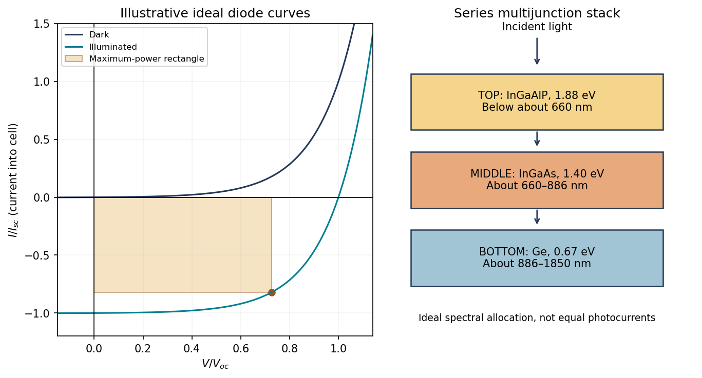
Original idealized photovoltaic current–voltage curves and the descending-bandgap order of the proposed three-junction stack
. Details. 
The solar-cell fill factor compares maximum delivered power with the open/short-circuit rectangle:Series resistance, leakage, recombination and temperature change the shape and hence the fill factor. Neither the short-circuit nor the open-circuit point itself delivers power.
The useful bandgap depends on the illumination spectrum, not only on whether the device is indoors or outdoors. The stipulated gap gives a long-wavelength absorption threshold near ; gives about using in nanometers.
Outdoor sunlight contains substantial visible and near-infrared power, so cadmium telluride can use a broader portion of that spectrum while retaining a useful output voltage. Its direct-gap absorption permits thin absorbers and large-area thin-film manufacture. Challenges include contacts and interfaces, collection and recombination, material supply and managing cadmium-containing material through fabrication and end-of-life handling.
Many indoor lamps concentrate their emission in the visible and provide little near-infrared power. A wider-gap absorber can then trade fewer lost useful photons for a higher attainable voltage and a smaller thermal dark-current penalty. Hydrogenated amorphous silicon has strong visible absorption, permits low-temperature large-area deposition and can suit low-power indoor devices. Disorder and defects restrict transport, and light-induced degradation and passivation stability must be controlled. Its larger gap forfeits more of the outdoor red/near-infrared spectrum.
These are suitability arguments, not guaranteed efficiencies. Indoor lamp spectra differ, and shunt leakage and recombination become particularly important at low light. Bandgap alone does not establish which finished device produces more power in every room.
For a monolithic series-connected multi-junction solar cell, all junctions carry the same terminal current, so a weakly illuminated junction limits the useful series current. Adjust absorber thicknesses, compositions and optical coupling to balance collected photocurrent. Tunnel interconnects provide electrical continuity; low-loss contacts and interfaces also matter. Equal incident energy in each spectral band would not guarantee equal current, because photon counts and collection efficiencies differ.
Put the largest bandgap at the illuminated top and the smallest at the bottom:The top absorber captures high-energy photons while transmitting lower-energy photons to the subsequent layers. Placing germanium first would absorb photons that the higher-gap cells could use at higher voltage.
The absorption edges are approximatelyFor ideal sharp, complete absorption without reflection, the available plotted spectral bands are therefore the visible region below for the top cell, – for the middle cell, and – for germanium. Photons beyond pass all three ideal absorbers. The source plot begins around , so it does not supply an ultraviolet integral below that point.
Using coarse readings of the provided curve, the band integrals are of order , and in plotted-ordinate-units times nanometers, respectively. These are only approximate areas under a low-resolution graph, not calibrated radiances in SI units: the ordinate gives no physical unit or spectral normalization. The robust result is the band allocation; precise photocurrent matching needs a calibrated spectrum and each junction's external quantum efficiency,Thus the diagram and band boundaries establish the intended stack, while the plot cannot justify precise watt-per-area or current values.
The dimensional material figure of merit and its common dimensionless form areHere is the Seebeck coefficient, the electrical conductivity, the electrical resistivity, and the total thermal conductivity. has units ; is dimensionless.
Seek a large thermoelectric power factor and low thermal conductivity. Optimize carrier concentration and band structure to balance thermopower and conductivity. Alloy disorder, complex unit cells, grain boundaries or suitable nanoscale features can scatter phonons and reduce lattice heat transport.
The properties are coupled: increasing carrier density often reduces , electronic heat conduction grows with electrical transport, and boundaries that scatter phonons may also scatter carriers. Evaluate the net change and the operating-temperature range, rather than maximizing each favorable term independently.[ref]
Complex thermoelectric materials by G. Jeffrey Snyder and Eric S. Toberer. Carrier-concentration tradeoffs and strategies for reducing lattice heat transport
Conducting organic materials can be attractive for flexible, lightweight and near-ambient heat harvesters; inorganic materials offer a wider established range of high-performance and high-temperature options. The appropriate comparison includes device geometry and durability as well as peak .
Conducting polymers can have low lattice thermal conductivity, be solution processed and accommodate mechanically compliant large-area devices. Their carrier concentration and ordering can be modified through doping and processing. Contact resistance, environmental stability, reproducibility and obtaining stable complementary p- and n-type materials can limit practical modules. Their organic character does not imply that they remain stable at high temperature.
Inorganic thermoelectrics can provide high power factors, temperature stability and mature transport data over application-specific ranges. Some compositions are brittle, dense, expensive or contain elements requiring careful environmental management; they are not all interchangeable. Interfaces, thermal cycling and interconnects can dominate device lifetime.
An experimental example of organic optimization controlled the oxidation level of a conducting polymer to balance transport and its low thermal conductivity, showing that organics are not categorically excluded from thermoelectric performance improvements.[ref]
Optimization of the thermoelectric figure of merit in PEDOT by Olga Bubnova and others. Nature Materials10, pp.429–433, abstract: oxidation-level control and low thermal conductivity
Material selection should use measured properties across the actual temperature interval and the achievable thermal gradient, not a blanket organic-versus-inorganic ranking. Articles by others on the same topic
There are currently no matching articles.