Take a p-n junction made from one semiconductor, with the p-type semiconductor on the left and the n-type semiconductor on the right. At thermal equilibrium the chemical potential is horizontal throughout. Before contact the chemical potential lies nearer the valence band on the p side and nearer the conduction band on the n side; after contact the band edges bend to permit one common value.
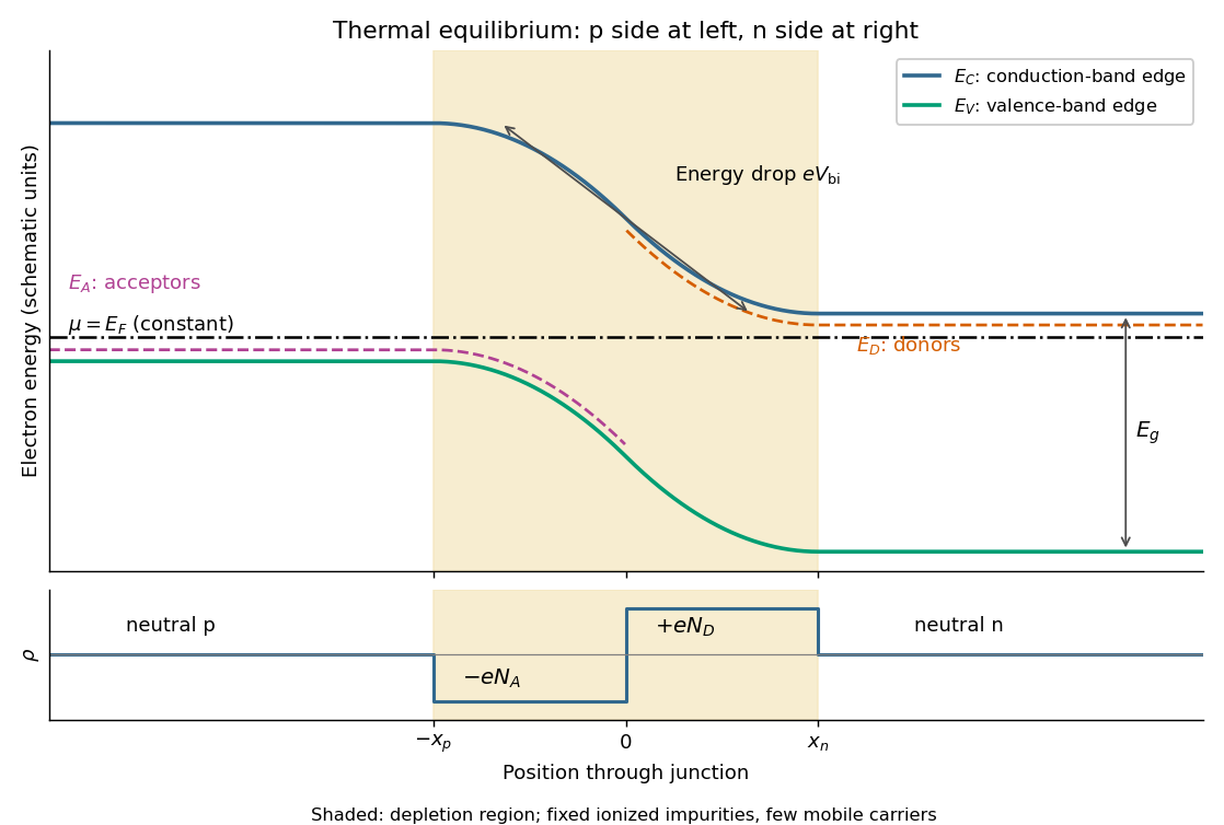
Original equilibrium p-n junction energy band diagram, impurity levels, common chemical potential and depletion region
. Details. 
In this orientation both the conduction band edge and the valence band edge decrease from p to n by . For a homojunction their separation is constant. The acceptor impurity level lies just above where acceptors are present, and the donor impurity level lies just below where donors are present. These impurity levels follow the local band bending; they do not form one additional horizontal band across the device.
The shaded depletion region has few mobile Electrons or electron holes and contains fixed negative ionized acceptor impurities on the p side and positive ionized donor impurities on the n side. Thus its electric field points from n to p. Its neutral outer regions have negligible electric field, so the band edges become flat there. In the depletion approximation, charge neutrality requires ; the symmetric drawing illustrates rather than assuming that equality is universal. Diffusion and field-driven drift current cancel at equilibrium: no applied voltage does not mean zero internal electric field or zero built-in electric potential difference.
Articles by others on the same topic
There are currently no matching articles.