Let the nearest-neighbour spacing be , so the primitive unit cell has length . Denote the two longitudinal displacements in cell by , with spring within each cell and spring between cells. Hooke's law and Newton's second law giveFor normal modes and , the two amplitudes satisfyIts vanishing determinant gives the alternating-spring chain dispersion relationThe minus sign is the acoustic phonon branch, with and at the origin. The plus sign is the optical phonon branch, with at the origin. For positive springs the acoustic phonon branch rises from zero to at the Brillouin zone edge; the optical phonon branch falls from to . Their long-wavelength limits areThus the leading frequency in the strong-bond limit of the alternating-spring chain is , the internal stretching frequency of a pair with reduced mass .
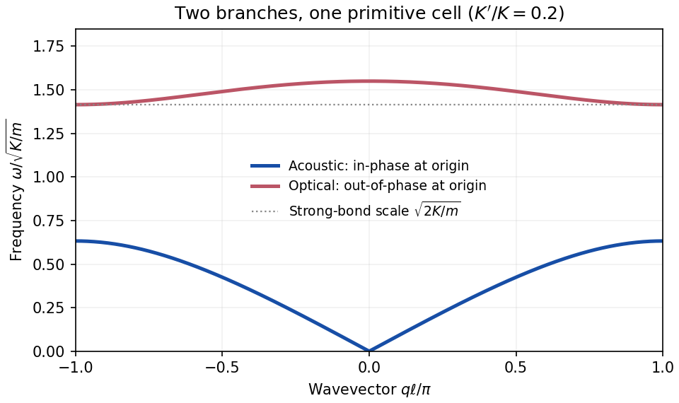
Acoustic and optical branches of an alternating-spring chain
. Original calculated dispersions for , using the two-atom primitive cell. Frequencies are in units of . Details.
A positive gate voltage attracts Electrons towards the oxide interface of the p-type semiconductor and repels mobile electron holes. The uncovered ionized acceptors form a negatively charged depletion region. Increasing the voltage further creates a thin electron-rich semiconductor inversion layer at the surface. The conduction band and valence band both bend downwards towards the positively biased gate, because an electron's electrostatic energy is .
In an ideal nondegenerate substrate with acceptor density , write and surface potential relative to the neutral bulk. The electron and hole surface densities areThe first change of majority-carrier type occurs at , where . The conventional MOS inversion threshold for appreciable strong inversion isAt threshold the inversion sheet is just developing, while a much thicker depletion region lies between it and the neutral p-type bulk. Inversion does not require the conduction band to cross the Fermi level: the surface can remain nondegenerate.
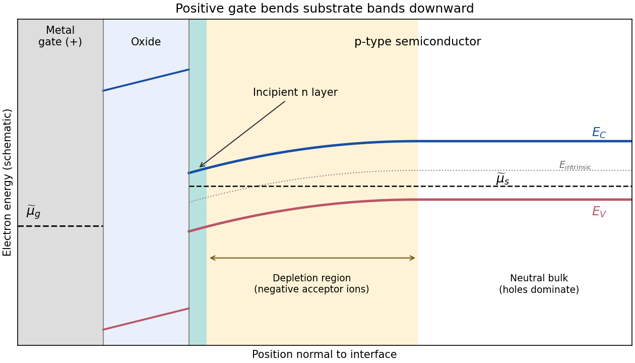

The metal and semiconductor Fermi levels need not be equal. The ideal oxide blocks particle exchange, so the gate and substrate can maintain different electrochemical potentials. In a biased MOSFET, the gate-to-substrate Fermi-level difference is , when the applied voltage is defined in the electron-reservoir convention. Each region can separately be in internal equilibrium. If an external zero-voltage connection instead equilibrates the reservoirs, their Fermi levels coincide, but different work functions can still cause band bending. Here the chemical potential shown in a band diagram is the electron electrochemical potential; the purely chemical contribution alone is not the equilibrium criterion for charged particles.
For a single carrier species with positive charge carrier mobility , the Hall coefficient and longitudinal electrical conductivity areTake the electric current density along , magnetic field along , and no transverse current. Then and , giving the Hall angle relationThe sign specifies the electron Hall polarity; the ratio of field magnitudes is . Converting the stated electron mobility to SI gives . ThereforeThis uses the homogeneous single-carrier Drude model; the carrier density cancels.
Articles by others on the same topic
There are currently no matching articles.