The following original schematic shows the two data organisations. Register-address, write-enable and memory controls are common background; the diagram highlights the changed combinational logic paths.
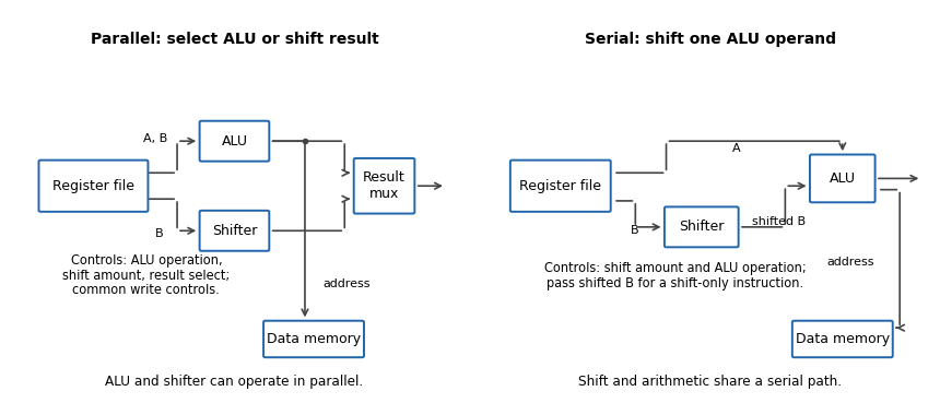

In the parallel design the result-source multiplexer selects either the arithmetic logic unit or barrel shifter. Its control is additional to the ALU function and shift amount. (i) Addition: read the two operands, select ALU addition and select the ALU result; the shift amount is irrelevant. (ii) Constant left bit shift: read the operand to be shifted, set the shift amount from the immediate operand and select the barrel shifter result; the ALU operation is irrelevant.
In the serial design the result comes through the ALU, so that result-source selection disappears. Its shift-amount control is now relevant to arithmetic as well. (i) Addition: set the barrel shifter to zero shift and select ALU addition, so its inputs are the unshifted processor register values. (ii) Constant left bit shift: set the requested shift and select an ALU operation that passes the shifted operand through. If the ALU lacks that operation, implement it or provide a selectable zero on its other input and add zero. This requirement should be stated, rather than assuming that an ordinary two-input add automatically performs a shift alone.
The ALU result can still supply the memory address. For a register-result instruction, enable processor register writeback and leave memory writes disabled. If the ISA requires shift carry flags, the flag-generation control must retain the barrel shifter's outgoing-bit information; blindly using a pass-through ALU's arithmetic carry is insufficient.
Articles by others on the same topic
There are currently no matching articles.