Topics (349k) Articles (361k) Users (423) Discussions (237) Comments (383) Files (12k) New article
Condensation followed by gravitational settling removes chemical elements from an atmospheric layer. The remaining gas may be in local chemical equilibrium with a depleted elemental inventory, while the column is not a closed equilibrium system.
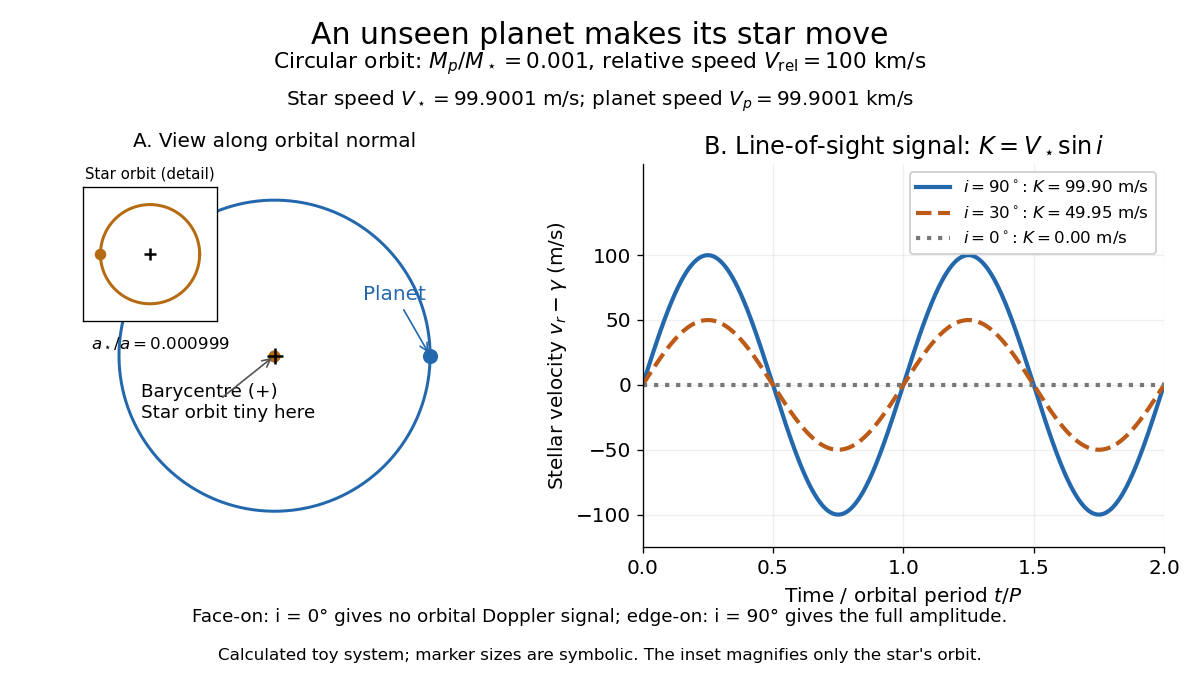
Doppler spectroscopy detects an exoplanet through the host star's changing Doppler shift. Both bodies orbit their shared astronomical barycenter: the star undergoes stellar reflex motion even when the exoplanet itself is unseen. Its velocity along the line of sight shifts its spectral lines; at speeds small compared with the speed of light, , with positive for recession. Repeated measurements can fit a Kepler orbit, rather than merely detect one shifted spectrum. Starspots and other changes in stellar spectral lines must be distinguished from actual orbital motion.
For one companion in an isolated two-body problem, the stellar radial-velocity semi-amplitude isHere is the gravitational constant, the orbital period, the orbital eccentricity, and the star and exoplanet masses. The orbital inclination is measured relative to the sky plane: is face-on and is an edge-on orbit. The exact binary mass function measured from the fitted orbit isWith known and , this is usually reported as . Taking gives the minimum companion mass; a smaller orbital inclination allows a larger mass. A detected exoplanet transit constrains close to for a compact planet orbiting well outside the star's surface, substantially resolving this ambiguity. Combining Doppler spectroscopy and exoplanet transit photometry then supplies a mass and radius for exoplanet interior studies.
For a computed circular example, let and choose a relative orbital speed : this is the speed of the planet relative to the star, not its speed about the astronomical barycenter. Conservation of momentum givesThe barycentric velocities point in opposite directions, so their speeds add to . Here and : at , at , and zero at . The star still orbits in the face-on case, but its orbital velocity has no line-of-sight component. The plotted circular signal is for a chosen phase origin and constant system velocity .
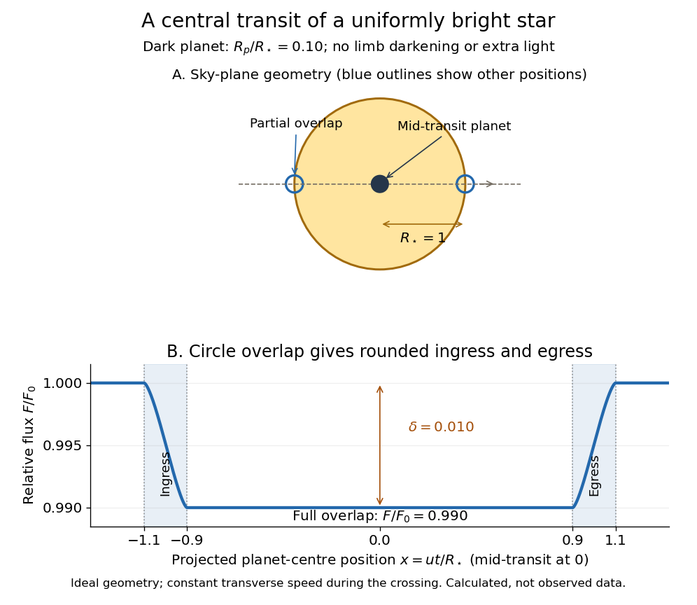
Exoplanet transit photometry measures the decrease in a star's observed radiative flux during an exoplanet transit. Define as the unobscured star's observed radiative flux and as the value at time . For a dark, opaque exoplanet crossing a uniformly bright circular stellar disc, a fully superimposed planetary disc blocks exactly the fractionHere and are the planet and star radii. This exoplanet transit depth determines a radius ratio, ; an absolute planet radius requires an independently estimated stellar radius. For , : a one-percent dip, with . Halving the radius ratio to reduces the exoplanet transit depth to , a quarter as much.
For the central exoplanet transit illustrated below, the transit impact parameter is . Write and let be the projected centre-to-centre separation in units of . The light curve is , where is the overlap area of circles of radii and . There is no overlap when ; the planetary disc is fully inside when , giving . Between those limits, the overlap area grows or shrinks continuously. Thus even a uniform star has curved ingress and egress, with a flat bottom only during full overlap. The illustration uses approximately constant transverse velocity over the short crossing, so with mid-transit at . Analytic models also handle limb darkening. [ref]
https://arxiv.org/abs/astro-ph/0210099. Mandel and Agol (2002)
.
The simple exoplanet transit depth formula assumes constant stellar brightness, no limb darkening or starspots, negligible light from the exoplanet, and no transit dilution by other light. It describes full overlap in a non-grazing exoplanet transit, requiring for a full-overlap interval. A grazing exoplanet transit never hides the whole planetary disc against the star, and limb darkening weights different blocked areas differently. Repeating dips are valuable evidence, but eclipsing binary stars and starspots can imitate parts of the signal, so confirmation and joint modelling matter.
An exoplanet thermal phase curve measures infrared brightness throughout the orbit. Its amplitude constrains day-night heat redistribution, while its maximum's displacement from secondary eclipse constrains the offset of the hottest atmospheric region. Wavelength-dependent opacity makes different channels probe different pressures.
The atmospheric advection time over length at wind speed is . Day-night heat redistribution tends to be efficient when this time and the relevant wave-adjustment time are shorter than the radiative relaxation time in a planetary atmosphere.
A column near pressure contains mass per area of order . Linearizing its blackbody cooling around temperature gives the estimatewhere is specific heat capacity at constant pressure. This estimate omits details of wavelength-dependent radiative transfer, but captures faster relaxation in hotter and lower-pressure atmospheric layers.
For an integer-valued underlying with European call option prices , the second strike difference equals . It is the discrete counterpart of recovering a payoff probability distribution from strike derivatives.
For a martingale with increments in , European call option prices satisfy . At positive-probability states, the variance and the upward/downward conditional transitions are determined by this identity; transitions at zero-probability states cannot be recovered.
The Mellin transform of call prices can be inverted along a vertical contour with real part : . A finite exponential moment at and the quadratic denominator give absolute convergence.
A sequence in is equidistributed if the limiting frequency in every half-open interval equals that interval's length. Equivalently, its empirical probability measures converge to normalized Lebesgue measure when tested against every continuous function.
For a bounded sequence in a Hilbert space, put . If , then in norm. Since the are bounded, it suffices that has convergence in density of a sequence to zero. The proof applies the Cauchy-Schwarz inequality to an average of shifted sums.
A continuous self-map of a compact metric space is uniquely ergodic when it has exactly one invariant Borel probability measure. An irrational rotation of the circle is uniquely ergodic: invariance multiplies its nonzero-index Fourier coefficients by nontrivial phases, forcing those coefficients to vanish. The Stone-Weierstrass theorem then identifies the invariant measure as normalized Lebesgue measure.
Cutting and stacking constructs measure-preserving transformations from towers of equal-measure levels. Cut a tower into equal-width subcolumns, add new spacer levels, and stack the resulting columns. Map each level to the one above by a measure-preserving identification; subsequent stages extend the partial map. When uncovered and top-level measures tend to zero, the limiting map is defined modulo null sets.
For a measurable transformation , a measure is invariant if the pushforward measure equals the original measure, or equivalently for every measurable . This is the measure used in a measure-preserving system.
High-minimum-degree multipartite stability subgraph by  Codex 0 Created 2026-10-05 Updated 2026-10-07
Codex 0 Created 2026-10-05 Updated 2026-10-07For fixed positive integers , a graph on vertices with and no balanced complete multipartite blow-up contains an -partite subgraph with vertices, balanced classes of size , and minimum degree of a graph .
One proof first removes a vanishing fraction of vertices of low degree of a vertex, finds a slowly growing by the Erdős-Stone theorem, and assigns almost every remaining vertex to a root class in which it has fewer than neighbours of a vertex. After discarding a further vanishing fraction, a inside an assigned class would extend to using the root classes. Thus internal edges and missing cross-class edges both number . Removing the vertices with unusually many missing cross-class edges gives the stated minimum degree of a graph.
An equivalence class collects all the set elements indistinguishable from a specified set element under an equivalence relation. For an equivalence relation on a set , the precise definition isThe ambient set matters: a finite class for integer congruence restricted to differs from the infinite residue class for the same integer congruence on all integers. We write when the equivalence relation and ambient set are clear.
In the finite modulo-three example,There are nine names but only three distinct equivalence classes. In particular, , whereas : the first statement is membership of a set element; the second is equality of two sets.
For any equivalence relation on , the essential rule isReflexivity puts in , so the equivalence classes are nonempty and cover . If two equivalence classes share , the symmetric relation property and transitivity relate their defining elements through ; transitivity then makes their members coincide. Thus distinct equivalence classes are disjoint, giving a partition of a set. Conversely, declare two set elements equivalent when they belong to the same block of a partition of a set. The three relation properties follow immediately and its equivalence classes recover the blocks. [ref]
https://www.math.umd.edu/~pbrosnan/notes/ugalg/sect0018.html. Patrick Brosnan, Undergraduate Algebra, §2.10, Lemma 2.81, Corollary 2.82 and Theorem 2.83
Equivalence of partial functions modulo finite changes by Codex 0 Created 2026-10-05 Updated 2026-10-07
Codex 0 Created 2026-10-05 Updated 2026-10-07Two functions and , whose domains lie in one ambient set, are equivalent modulo finite changes when is a finite set and the functions disagree at only finitely many points of . The symmetric difference inclusion handles domains in a transitive chain. An exceptional set for values must also include points of absent from the middle domain ; these lie in the finite difference .
For fixed positive frequency and , the equatorial shallow-water dispersion relation has real zonal wavenumbers only ifBetween these values the zonal roots are complex, giving an evanescent response rather than freely propagating modes.
For epicyclic motion in a Keplerian shearing sheet, write . The energy of the radial harmonic oscillator per unit mass is . The full horizontal Jacobi energy in a shearing sheet also includes the negative guiding-center term .
Pinned article: Introduction to the OurBigBook Project
Welcome to the OurBigBook Project! Our goal is to create the perfect publishing platform for STEM subjects, and get university-level students to write the best free STEM tutorials ever.
Everyone is welcome to create an account and play with the site: ourbigbook.com/go/register. We belive that students themselves can write amazing tutorials, but teachers are welcome too. You can write about anything you want, it doesn't have to be STEM or even educational. Silly test content is very welcome and you won't be penalized in any way. Just keep it legal!
Intro to OurBigBook
. Source. We have two killer features:
- topics: topics group articles by different users with the same title, e.g. here is the topic for the "Fundamental Theorem of Calculus" ourbigbook.com/go/topic/fundamental-theorem-of-calculusArticles of different users are sorted by upvote within each article page. This feature is a bit like:
- a Wikipedia where each user can have their own version of each article
- a Q&A website like Stack Overflow, where multiple people can give their views on a given topic, and the best ones are sorted by upvote. Except you don't need to wait for someone to ask first, and any topic goes, no matter how narrow or broad
This feature makes it possible for readers to find better explanations of any topic created by other writers. And it allows writers to create an explanation in a place that readers might actually find it.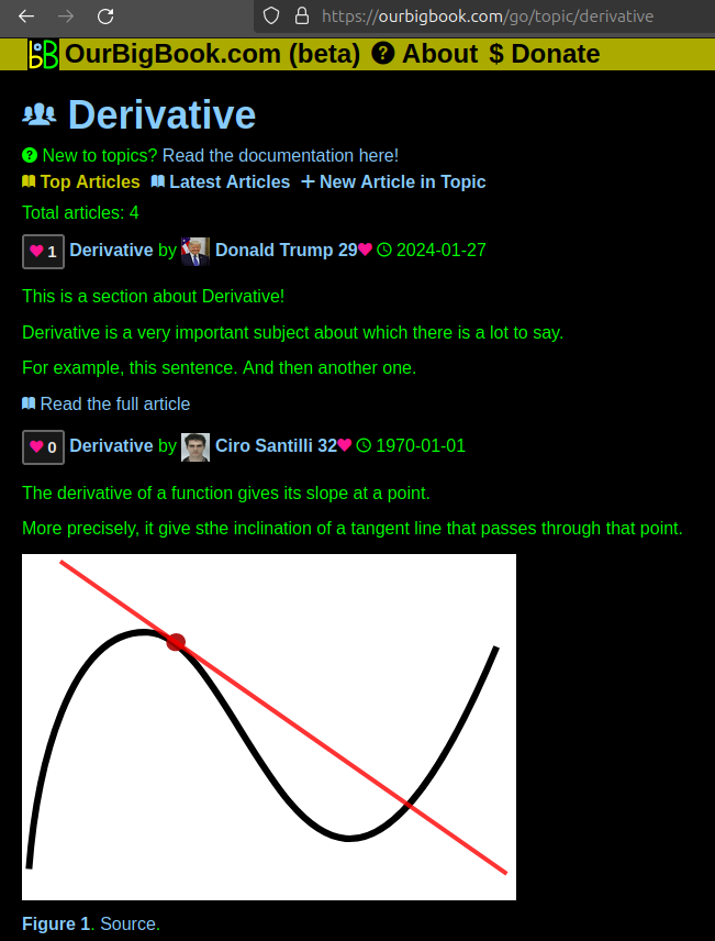
Figure 1. Screenshot of the "Derivative" topic page. View it live at: ourbigbook.com/go/topic/derivativeVideo 2. OurBigBook Web topics demo. Source. - local editing: you can store all your personal knowledge base content locally in a plaintext markup format that can be edited locally and published either:This way you can be sure that even if OurBigBook.com were to go down one day (which we have no plans to do as it is quite cheap to host!), your content will still be perfectly readable as a static site.
- to OurBigBook.com to get awesome multi-user features like topics and likes
- as HTML files to a static website, which you can host yourself for free on many external providers like GitHub Pages, and remain in full control

Figure 2. You can publish local OurBigBook lightweight markup files to either OurBigBook.com or as a static website.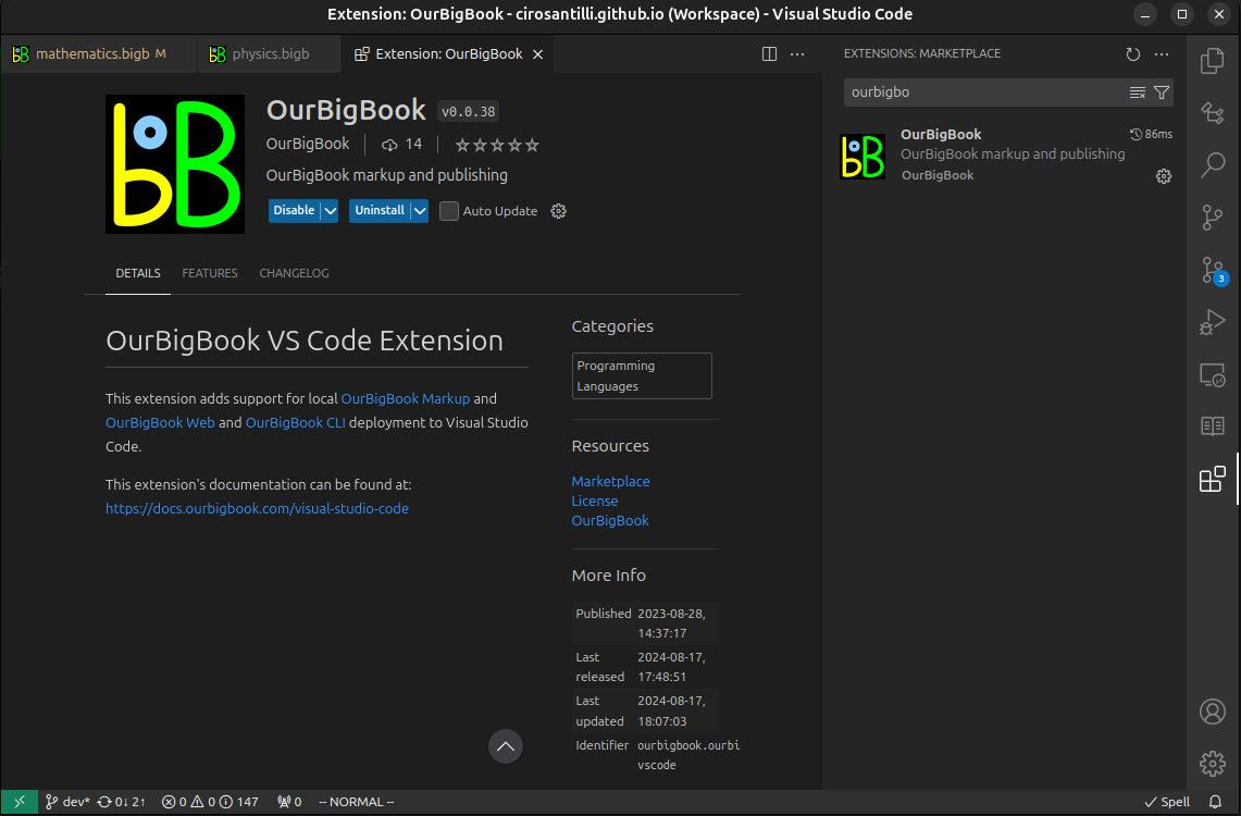
Figure 3. Visual Studio Code extension installation.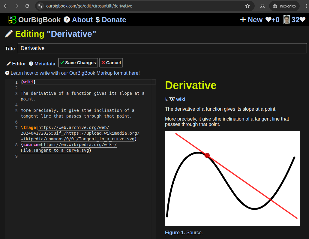
Figure 5. . You can also edit articles on the Web editor without installing anything locally. Video 3. Edit locally and publish demo. Source. This shows editing OurBigBook Markup and publishing it using the Visual Studio Code extension. 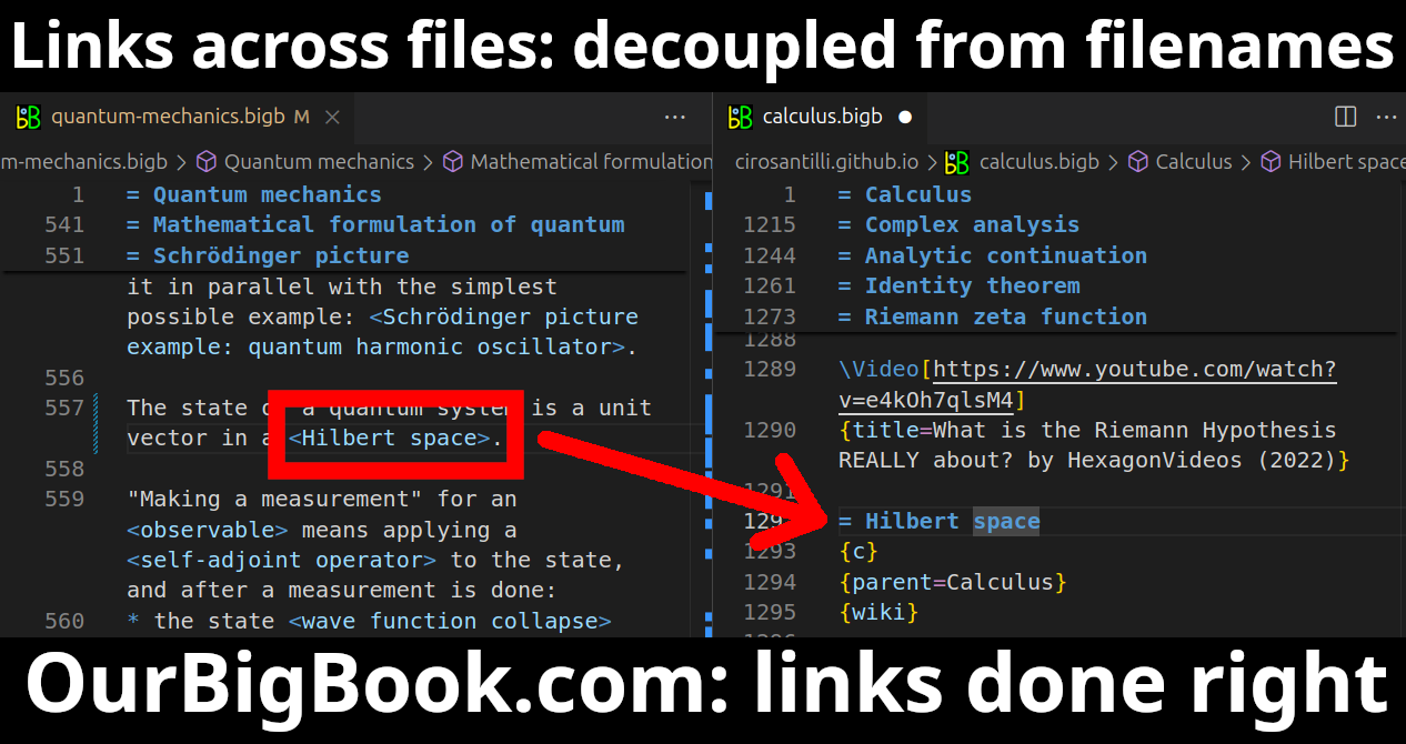
- Infinitely deep tables of contents:
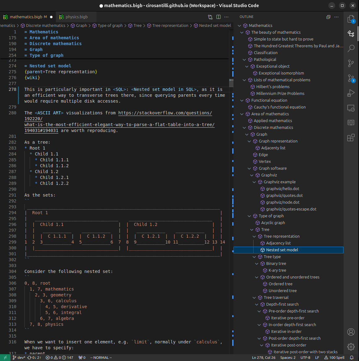



All our software is open source and hosted at: github.com/ourbigbook/ourbigbook
Further documentation can be found at: docs.ourbigbook.com
Feel free to reach our to us for any help or suggestions: docs.ourbigbook.com/#contact