For parabolic bands, the density of states near a subband edge scales as , , and . Thus a quasi-1D wire has inverse-square-root singularities at successive transverse subband thresholds, a quasi-2D well has a staircase, and a bulk 3D band rises smoothly from zero. Each expression vanishes below its threshold.
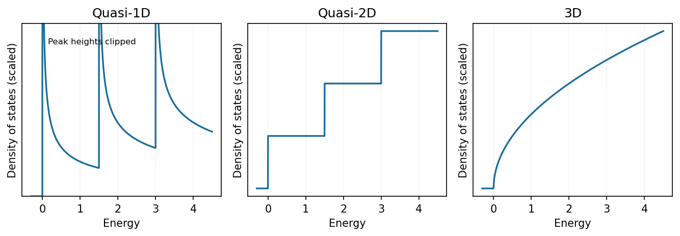
Parabolic-band density of states in one, two and three unconfined dimensions
. Source. Details. 
These sketches assume extended noninteracting states with simple quadratic dispersion. Finite temperature, disorder and finite lifetime broaden measured threshold features; the ideal singularity is integrable and does not represent infinitely many states in a finite energy interval.
n-type doping adds donor impurities with weakly bound electrons near the conduction-band edge; ionization supplies conduction electrons and leaves positive donor ions. p-type doping introduces acceptors near the valence-band edge, producing holes and negatively charged ionized acceptors. Silicon and germanium commonly use group-V donors and group-III acceptors; dopant behaviour in a compound semiconductor depends on its lattice site.
Doping sets carrier concentration, Fermi level and resistivity. Spatially patterned donor and acceptor regions form p-n junctions, transistor source/drain regions and electrical contacts; remote doping can supply carriers to a cleaner conducting layer. Compensation and incomplete ionization mean carrier density need not equal the total impurity concentration.
A larger-gap AlGaAs barrier has a higher conduction-band edge than GaAs. Donors in AlGaAs supply electrons that transfer into lower-energy GaAs states, leaving a positively charged donor region. The resulting electrostatic field bends the GaAs conduction band into a triangular interface well. Motion normal to the interface is quantized, while motion parallel to it remains approximately free, producing a two-dimensional electron gas.
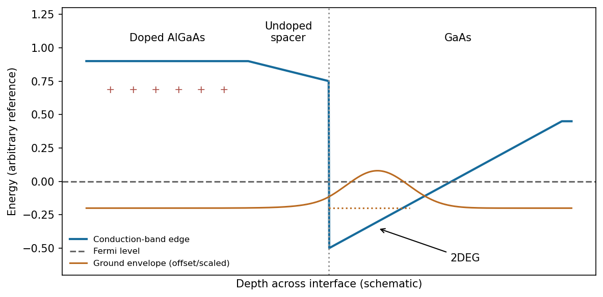
An illustrative remotely doped heterojunction separates the electron envelope from ionized donors
. Source. Details. 
The confined envelope peaks just inside GaAs and decays into the AlGaAs barrier; a triangular-well treatment gives an Airy-function-like envelope with boundary matching. An undoped spacer separates the electrons from the donors, strongly reducing ionized-impurity scattering compared with uniformly doped 3D material and enabling high mobility. Band offsets, donor supply, interface roughness and electrostatics jointly determine whether a single occupied subband is obtained.
For longitudinal motion in transverse subband ,For a completely free particle take and use the full wave vector. In a semiconductor the parabolic-band mass is the appropriate effective mass rather than necessarily the bare electron mass.
For a wire of length , one spin state has states in one propagation direction. Including two degenerate spin states and using givesDivide by for density per unit length. The factor-of-two distinction is essential: the current from one reservoir uses only its incoming propagation branch. If spin degeneracy is lifted, count each resolved spin channel separately.
Use the one-way density per unit length . The electron-flux magnitude in an interval is charge times velocity times line density:If is instead defined for a finite length , the traversal frequency is ; the same cancellation follows. The printed therefore requires to be a line density, not an unscaled total particle number.
Subtract the opposite reservoir's incoming flux. With the stated electron electrochemical potentials, conventional positive current is opposite to electron-number flux, soAt low temperature and small bias, each fully transmitted occupied spin-degenerate subband contributes . Hence . More generally, the Landauer formula weights each mode by its transmission probability; imperfect transmission removes exact integer plateaux.
With ballistic conductance quantization, as a gate opens the channel, conductance plateaux at appear; successive transverse modes add one quantum, approximately per spin-degenerate subband. Their appearance is the key low-temperature electrical signature.
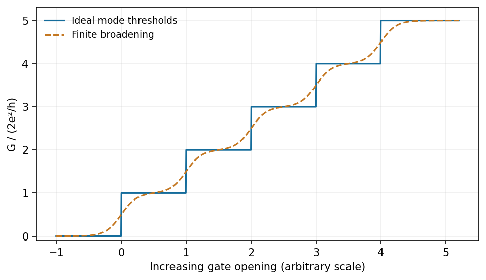
Ideal conductance plateaux sharpen as thermal and disorder broadening become small compared with subband spacing
. Source. Details. 
Require transverse confinement with separated subbands, and measurement-bias energy well below the subband spacing, a mean free path exceeding the channel length, and smooth low-reflection coupling to reservoirs. Correct for appreciable external series resistance. Phase coherence is needed for additional interference oscillations, but perfect phase coherence across an entire macroscopic circuit is not a separate requirement for the basic mode-counting result. A field that resolves spin splitting can produce increments.[ref]
Quantized conductance of point contacts by B. J. van Wees and others. Gate-controlled ballistic GaAs-AlGaAs point contacts and conductance steps
Articles by others on the same topic
There are currently no matching articles.