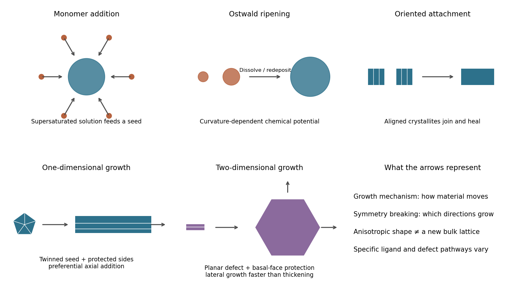
Three useful growth mechanisms are monomer addition, Ostwald ripening and oriented attachment. They can occur sequentially or compete; they are not necessarily three distinct experimental recipes.
In monomer-addition crystal growth, dissolved atoms, ions or molecular growth units attach to an existing nanocrystal. Supersaturation provides a chemical-potential driving force, approximately for an ideal solution. Transport through solution and incorporation at steps or facets determine the rate. Growth consumes the excess solute without requiring collisions between whole crystals.
In Ostwald ripening, smaller crystals dissolve while larger ones grow through solution. Curvature raises the surface contribution to chemical potential, approximately for a sphere with surface free energy and atomic volume . Dissolved material therefore moves from high-curvature particles to lower-curvature ones, reducing total interfacial free energy.
In oriented attachment, whole crystallites align compatible lattice planes and join. Removing exposed surface and forming a coherent interface lowers free energy; rotation, ligand removal and interface healing can be rate limiting. Misalignment can leave twins or other defects. Simple aggregation without crystallographic registration is related particle attachment, but is not necessarily oriented attachment.

Symmetry breaking in nanocrystal growth makes growth rates along initially equivalent crystallographic directions unequal, so the final shape has lower symmetry than an unperturbed seed. It need not change the underlying face-centered cubic lattice. A cubic lattice does not require a cubic external shape.
Anisotropy can originate in a twin or stacking fault, unequal ligand coverage of nominally equivalent sites, selective adsorption or etching, a substrate or external field, or a local fluctuation amplified because newly deposited material changes subsequent growth. Facet-selective binding suppresses some normal growth rates; concentration and reduction kinetics determine whether atoms can redistribute towards a near-equilibrium shape or remain in a kinetically selected one. A facet with slow normal growth tends to remain exposed, while a fast-growing facet can disappear.
For a one-dimensional silver example, begin with a small seed with multiple regions related by crystal twinning containing five sectors around a common axis. Ligand-protected lateral faces and more active ends favour axial addition, producing an elongated pentagonal rod and then a wire. The defect geometry and surface kinetics jointly distinguish the axial direction. Fivefold twinning is a composite structure with strain accommodation, not a perfect single fcc crystal with forbidden fivefold lattice symmetry.
For a two-dimensional example, begin with a seed containing a planar twin or stacking fault. Basal-face protection and enhanced incorporation at suitable edges favour lateral extension over thickening, producing a thin triangular or hexagonal plate. The accompanying schematic emphasizes seed, symmetry-breaking event and anisotropic growth stages. These are representative routes, not universal requirements for every rod or plate. Experimentally, silver-seed growth can also be redirected into lower-symmetry forms by controlling reduction kinetics.[ref]
Symmetry Breaking during Seeded Growth of Nanocrystals by Xiaohu Xia and Younan Xia. 2012, seeded-silver growth and kinetic symmetry breaking
In surface-enhanced Raman spectroscopy, electromagnetic SERS enhancement comes from the strong local optical field near a plasmonic metal nanostructure. A localized surface plasmon resonance in gold or silver can increase both the field driving a molecular Raman transition and the coupling of its emitted light to the far field. A common estimate isoften summarized as an enhancement when pump and Stokes frequencies see similar responses. Sharp tips and narrow interparticle gaps can produce intense hot spots.
Chemical SERS enhancement changes the molecule's Raman polarizability through adsorption, electronic hybridization or a metal–molecule charge-transfer resonance. It is more sensitive to molecular identity and binding geometry than a purely electromagnetic field enhancement, and generally requires close contact.
Tune particle size, shape and gap geometry so that a plasmon resonance overlaps the excitation and Raman frequencies, and bring the target into the enhanced-field region. Reproducible adsorption sites, low fluorescence background and clean reference spectra are as important as a large local enhancement. A hot spot does not guarantee that a dilute sample occupies it; a detection limit cannot be computed from concentration alone. Au or Ag improve the signal per suitably located molecule, while sampling and background determine the practical limit.
In atomic layer deposition, expose the surface to a molybdenum precursor, purge unreacted precursor and volatile products, expose it to a sulfur reactant, and purge again. Each half-reaction should saturate the available reactive sites rather than continue indefinitely with dose. Repetition builds a molybdenum disulfide film, with nucleation, incubation and layer closure checked independently.
Self-limited surface chemistry is not the same as depositing exactly one complete crystal monolayer per cycle. A cycle may add only a fraction of a layer, and initially isolated islands can thicken before all bare substrate is covered. Reactions on hydroxylated silicon dioxide can also differ from those on the comparatively inert MoS basal surface. A precursor pair must actually show saturation under the chosen conditions; simply alternating gases is insufficient evidence of ALD.
In metalorganic chemical vapor deposition, metalorganic and sulfur-containing precursors are typically supplied simultaneously or with overlapping residence times, and film growth depends on decomposition, transport and surface reaction rates. Both methods involve chemistry, but ALD separates saturating half-reactions and purge steps. An ALD process need not use a metalorganic precursor, and pulsed CVD is not automatically ALD.
Potential advantages are reproducible thickness increments, large-area uniformity, conformal access to features and compatibility with moderate-temperature integration. Saturated exposure can make coverage less sensitive to small precursor-flux variations than an unsaturated deposition rate. The cycle count provides a useful process variable for matching an optical or electrical thickness target.
For a monolayer device, control of nucleation and coalescence is especially valuable, because excessive second-layer growth and uncovered patches both change the optical response. The advantages are conditional: a reliable ALD window and suitable precursor chemistry are required, and conformality does not imply a single-crystal film. Long exposure and purge steps reduce throughput, residual ligands or impurities can remain, and post-growth crystallization may require temperatures that the integrated device cannot tolerate.
Many independently oriented nuclei form on an amorphous support and then coalesce before they can become one large crystal. The SiO substrate provides no unique epitaxial orientation. At relatively low deposition temperature, short surface diffusion lengths and slow bond rearrangement restrict the distance over which deposited species can find a well-ordered configuration. Island collisions therefore leave grain boundaries; precursor residues and incomplete sulfurization can add disorder.
Raising temperature or annealing can improve crystallinity, but may conflict with the ALD reaction window, substrate compatibility or sulfur retention. Small grains are consequently a frequent process outcome, not a fundamental theorem that ALD can never form a well-ordered layer. A direct ALD experiment on SiO-covered wafers found nanocrystalline MoS by diffraction and electron microscopy, while demonstrating self-limited precursor exposure behaviour.[ref]
Wafer-scale, conformal and direct growth of MoS2 thin films by atomic layer deposition by Yujin Jang and others. 2016, SiO2 substrates, self-limited growth and nanocrystalline microstructure
The pressure is . The molecular arrival flux from an ideal gas isBecause the residual-gas composition, temperature and sticking probability are not specified, the answer is an order-of-magnitude monolayer-equivalent exposure time, not a unique coverage prediction. Take , a nitrogen-like molecular mass , and unit sticking probability. ThenUse the given molecular-layer scale as an approximate intermolecular spacing, giving . ThusFor , this is a few minutes; assuming instead sites gives about , the same rough scale. A clean-looking vacuum pressure does not imply a contamination-free surface. Desorption and a small sticking probability can greatly lengthen net accumulation, while residual water or hydrocarbons can dominate the chemistry. Full saturation in a site-blocking adsorption model is not exactly the same as one monolayer-equivalent incident fluence.
Use a thin, continuous cap of hexagonal boron nitride, preferably assembled without exposing the cleaned MoS surface to ambient contamination. It is chemically inert and relatively transparent in the visible range, and can isolate the film from adsorbing water, oxygen and hydrocarbons during optical measurements. A transferred sheet avoids depositing a strongly reactive precursor directly on the monolayer.
The cap must cover the illuminated region and overlap its edges; pinholes, wrinkles and unsealed edges can allow ingress. Trapped residues or bubbles can themselves change the optical response. Record the capped background and account for optical interference and dielectric-environment shifts rather than assuming that encapsulation leaves every spectral peak unchanged. A thin oxide or polymer coating may also provide protection, but deposition damage, optical background and permeability require checking. An atomically thin sheet with a perfect basal plane is not proof that the whole assembled enclosure is sealed.
Articles by others on the same topic
There are currently no matching articles.