Joining p-type and n-type regions initially allows majority carriers to diffuse across and recombine. Exposed negative acceptor charge on the p side and positive donor charge on the n side form a depletion region. Its electric field points from n to p and balances diffusion at equilibrium. The Fermi level is then spatially constant, while the conduction and valence band edges bend across the built-in potential; this equilibrium barrier cannot supply continuous power to a load.
forward bias makes p positive relative to n, reducing the barrier from to . electrons enter p material and holes enter n material, becoming minority carriers whose diffusion and recombination sustain the current. reverse bias enlarges the barrier and leaves a much smaller minority-carrier current until breakdown. The ideal diffusion model gives , the Shockley diode equation; depletion-region recombination, series resistance and breakdown limit this approximation. Minority-carrier injection on both sides is essential to the junction theory.[ref]
The Theory of p-n Junctions in Semiconductors and p-n Junction Transistors by William Shockley. 1949, pp.435–436: rectification, electron and hole currents, and injection
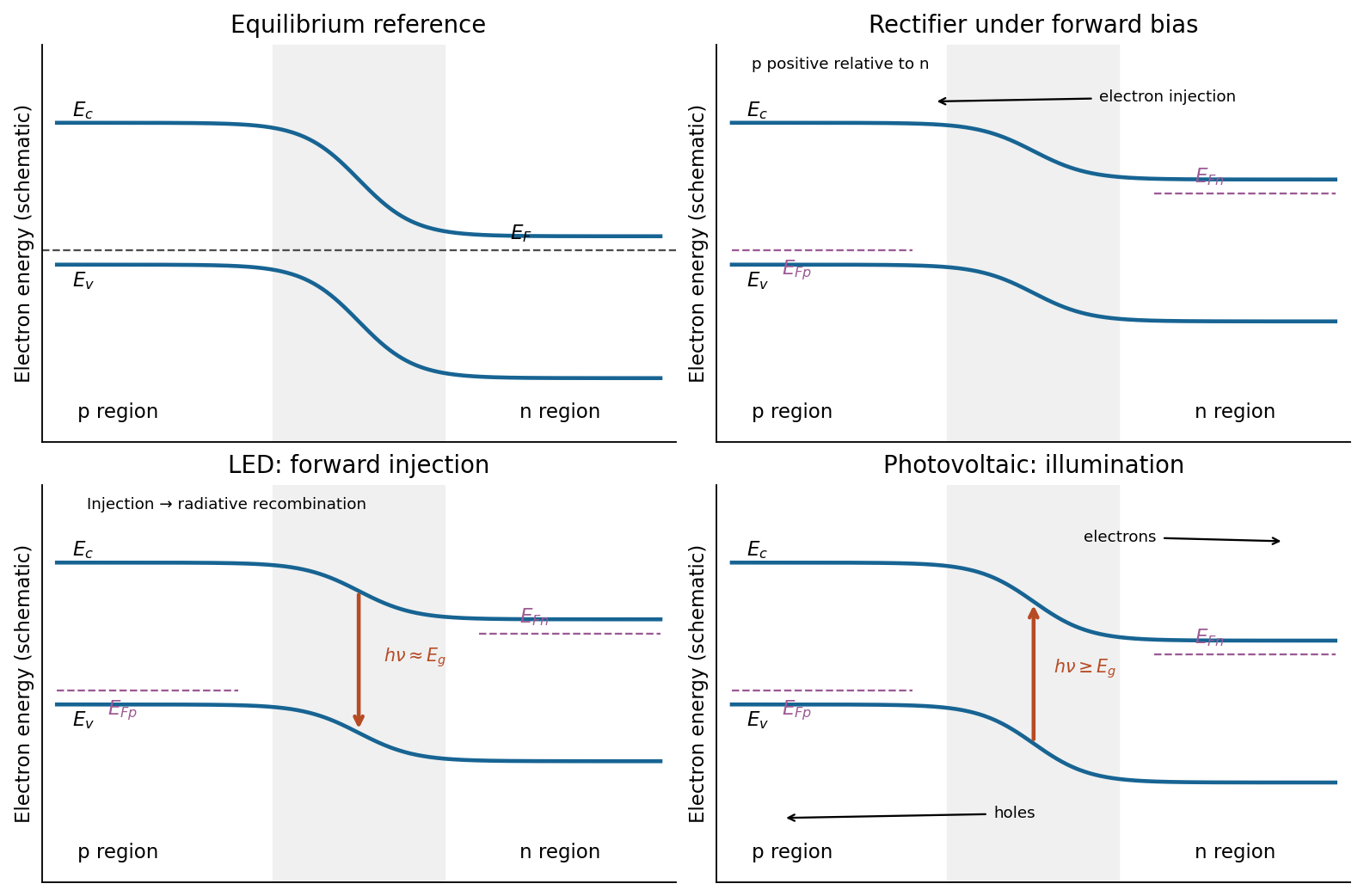
Junction band bending and three device functions
. Original schematic electron-energy diagrams, not quantitative band solutions. Equilibrium has one flat Fermi level; biased and illuminated panels indicate separate carrier quasi-Fermi levels. The photon arrows distinguish LED emission from solar-cell absorption. Details.
forward bias injects electrons and holes into a common active region. Their electron-hole recombination can emit a photon as an electron falls from a conduction-band state into an empty valence-band state, with approximately the band gap near the band edges. A direct band gap makes this radiative transition much more probable than an indirect gap requiring simultaneous phonon participation. Carrier confinement improves their overlap; nonradiative recombination and photon trapping reduce the external efficiency. This is spontaneous electroluminescence and does not require population inversion. The biased carriers have separate quasi-Fermi levels, rather than one global equilibrium Fermi level. The band-diagram downward arrow shows photon emission. As a concrete implementation, an InGaN/AlGaN double heterostructure was used for a bright blue junction LED.[ref]
Absorption of photons with creates electron-hole pairs, the upward band-diagram arrow. In the depletion region the built-in field drives electrons towards n material and holes towards p material; diffusion also delivers carriers generated within a diffusion length outside that region. Selective contacts collect the two signs. Illumination maintains a nonequilibrium quasi-Fermi-level splitting, allowing a voltage and useful current through an external load; it is the light, rather than the equilibrium barrier, that supplies the energy.
Taking forward diode current as positive, an ideal illuminated junction haspower is delivered where in this convention. Reflection, below-gap transmission, carrier thermalization, recombination and resistive losses limit real conversion; even an ideal single junction has radiative detailed-balance limits.[ref]
Detailed Balance Limit of Efficiency of p-n Junction Solar Cells by William Shockley and Hans-Joachim Queisser. 1961, Journal of Applied Physics 32, pp.510–519: radiative detailed-balance limit
Articles by others on the same topic
There are currently no matching articles.