For a CMOS inverter, connect one PMOS transistor from the positive supply to the output and one NMOS transistor from the output to ground; drive both gates with the input . When , the PMOS transistor conducts and the NMOS transistor is off; when , the reverse holds. Thus the output is , using two transistors.
For a four-input NAND gate, use four NMOS transistors in series between the output and ground, with gates . Use four PMOS transistors in parallel between and the output, with the same gate signals. The pull-down network conducts exactly when all four inputs are one; the pull-up network conducts whenever at least one input is zero. HenceAs usual for static CMOS, tie the NMOS transistor bodies to ground and the PMOS transistor bodies to .
Each parenthesized pair in the given Boolean function tests equality of two input bits:This is logical equivalence, or the two-input XNOR gate function. Thus is one whenever either input pair agrees. Generate the four complemented inputs with four inverters, and define the following NAND gate outputs:Feed these four outputs into a single four-input NAND gate. De Morgan's laws giveHere juxtaposition denotes logical conjunction. The construction uses only inverters, two-input NAND gates and one four-input NAND gate, as required.
The four CMOS inverters use transistors, the four two-input NAND gates use , and the four-input NAND gate uses . Therefore this particular design uses
A more economical static CMOS design follows from factoring the condition for . The output is low exactly when both input pairs disagree:Generate with four CMOS inverters. Write or for an NMOS transistor or PMOS transistor whose gate receives . In the following network expressions, a dash means a series connection and means a parallel connection.
Connect this eight-device pull-down network between and ground:The first parallel module conducts exactly when and the second exactly when . Their series connection therefore conducts precisely when should be zero.
By complementary CMOS network duality, connect this eight-device pull-up network between and :A PMOS transistor conducts when its gate is zero. Consequently the first upper branch conducts when , namely ; the second conducts when . Their parallel connection gives the required logical disjunction. For every stable binary input, exactly one of the pull-up network and pull-down network conducts.
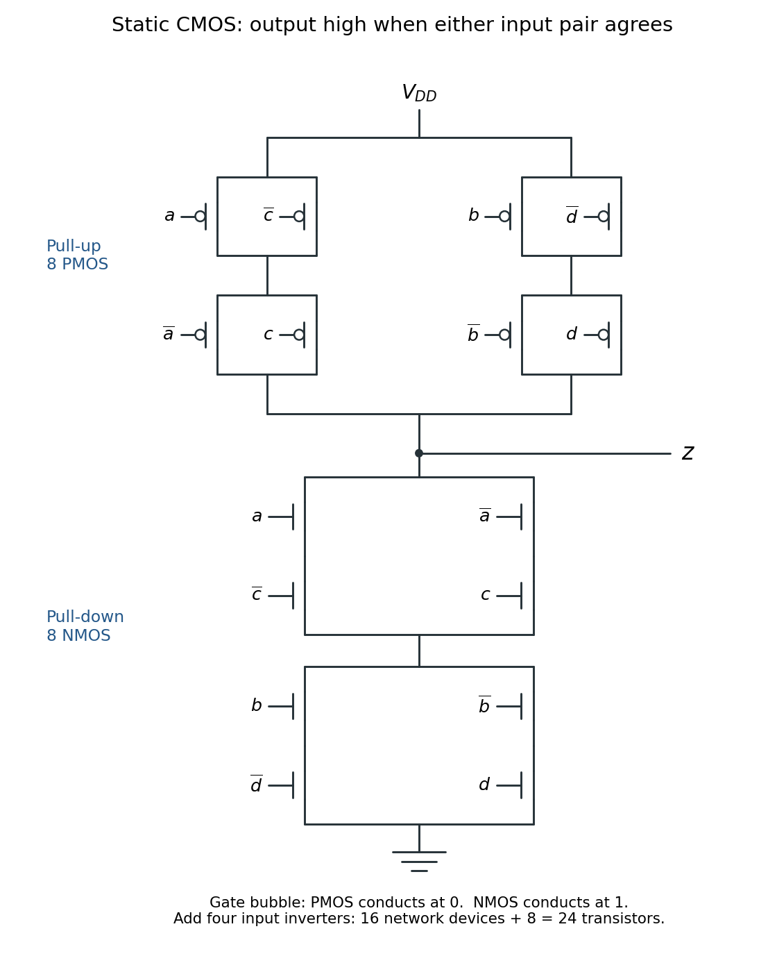
Complementary CMOS networks: eight PMOS transistors above the output and eight NMOS transistors below it
. Details. 
The figure labels each MOSFET channel by its gate signal; the four input CMOS inverters are additional to the devices drawn.
The custom CMOS circuit uses eight NMOS transistors and eight PMOS transistors in the output networks, plus eight transistors in the four input CMOS inverters:The complementary types give an actively driven output at either supply rail. An NMOS transistor provides a strong connection to ground; a PMOS transistor provides a strong connection to . An NMOS transistor used alone to pass a high level loses gate overdrive as the output rises, giving a threshold-degraded high level; the complementary problem affects a PMOS transistor passing a low level. Complementary networks avoid these degraded levels and, ideally, have no direct supply-to-ground conducting path for a stable input. Physical leakage and switching current remain, but a resistive load and its continuous static current are unnecessary.
Articles by others on the same topic
There are currently no matching articles.