Use three positive-edge-triggered D flip-flops, all driven by the same clock signal . Write the current binary representation as , with the least significant bit. The next state is the current value plus one when and minus one when , in each case modulo eight. A bit toggles under exclusive or with a one.
For upward counting, toggles when , while toggles when , the respective carry conditions. For downward counting the corresponding borrow conditions are and . Define the shared inverted direction and the two direction-match signalsEach is one exactly when : it equals for upward counting and for downward counting. Thus the Boolean functions for the three D inputs areImplement this with two NOT gates for , four two-input exclusive or gates for , and one two-input AND gate. Connect to the D flip-flop whose output is ; feed the three outputs back into the indicated gates. All three flip-flops capture simultaneously, so each equation uses the old state.
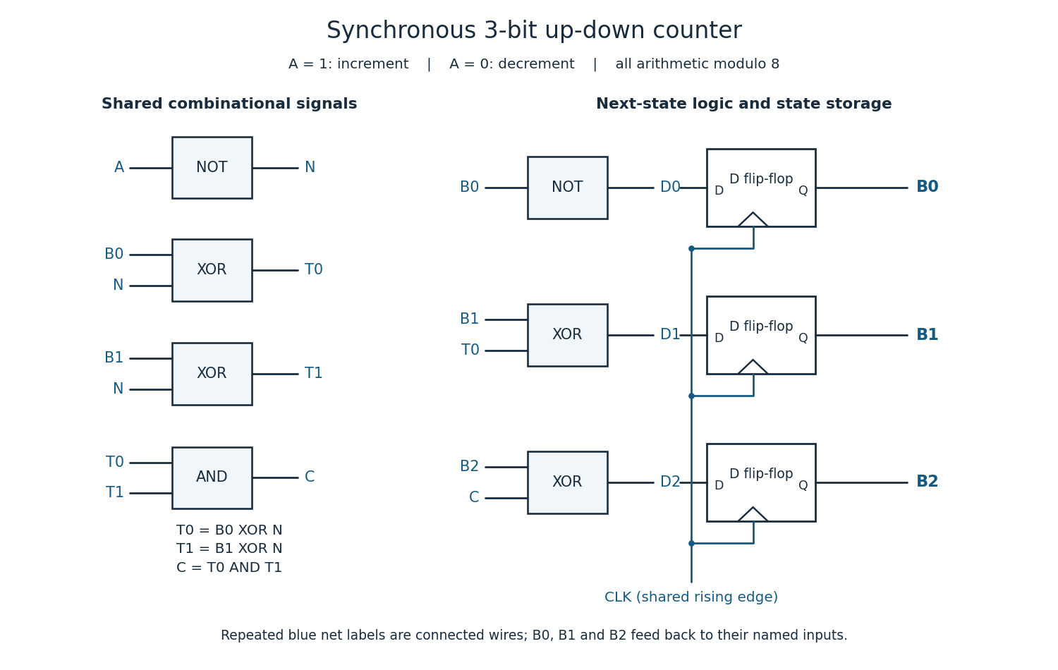

For completeness, the state transition table is
| Current | Next for | Next for |
|---|---|---|
000 | 001 | 111 |
001 | 010 | 000 |
010 | 011 | 001 |
011 | 100 | 010 |
100 | 101 | 011 |
101 | 110 | 100 |
110 | 111 | 101 |
111 | 000 | 110 |
Every three-bit state is valid. A reset may initialize the binary counter to zero if required; counting itself needs no extra state. The direction input must meet the setup time and hold time requirements at the active clock edge.
For an estimate, use the usual equal-device CMOS series-stack model: a -input NAND gate or NOR gate has a worst-case propagation delay approximately times that of an inverter, because a conducting path contains series transistors. An AND gate or OR gate adds an output inverter. With a 1 ns inverter this gives, for ,For it reproduces the stated 3 ns. This is a technology estimate under equal sizing and comparable loading, not a unique physical law inferable from a single measured delay. Actual propagation delay also depends on capacitance, fan-out and transistor sizing. If instead only the supplied two-input gates were allowed, a balanced tree would have worst-case depth and delay ns; that is a different construction from a single -input gate.
For the explicit circuit in part (a), the longest combinational logic path starts at , passes through the shared inverter, either direction-match exclusive or, the AND gate, and the final exclusive or feeding :The path takes 5 ns, the paths from or to take at most 7 ns, and takes 1 ns. Both direction-match exclusive or gates act in parallel; their delays are not added together. The 8 ns excludes clock-to-Q delay, setup time, hold time and clock-distribution effects, because the question asks only for the combinational logic delay.
Articles by others on the same topic
There are currently no matching articles.